DSE028N10N3 Datasheet. Equivalente. Reemplazo. Hoja de especificaciones. Principales características
Número de Parte: DSE028N10N3 📄📄
Tipo de FET: MOSFET
Polaridad de transistor: N
ESPECIFICACIONES MÁXIMAS
Pdⓘ - Máxima disipación de potencia: 312 W
|Vds|ⓘ - Voltaje máximo drenador-fuente: 100 V
|Vgs|ⓘ - Voltaje máximo fuente-puerta: 20 V
|Id|ⓘ - Corriente continua de drenaje: 170 A
Tjⓘ - Temperatura máxima de unión: 150 °C
CARACTERÍSTICAS ELÉCTRICAS
trⓘ - Tiempo de subida: 105 nS
Cossⓘ - Capacitancia de salida: 2710 pF
RDSonⓘ - Resistencia estado encendido drenaje a fuente: 0.0028 Ohm
Encapsulados: TO263
📄📄 Copiar
Búsqueda de reemplazo de DSE028N10N3 MOSFET
- Selecciónⓘ de transistores por parámetros
DSE028N10N3 datasheet
dsg030n10n3 dse028n10n3.pdf
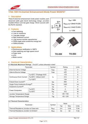
DSG030N10N3/DSE028N10N3 170A 100V N-channel Enhancement Mode Power MOSFET 1 Description These N-channel enhancement mode power mosfets used V = 100V DSS advanced splite gate trench technology design, provided 2 D excellent Rdson and low gate charge. Which accords with R = 2.6m TO-220 DS(on) (TYP) the RoHS standard. G R = 2.4m TO-263 DS(on) (TYP) 1 2 Features 3
dse026n10n3a.pdf
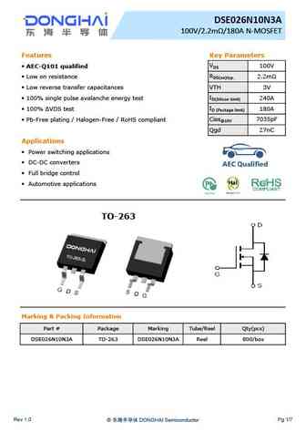
DSE026N10N3A 100V/2.2m /180A N-MOSFET Features Key Parameters VDS AEC-Q101 qualified 100V RDS(on)typ. Low on resistance 2.2m Low reverse transfer capacitances VTH 3V ID(Silicon limit) 100% single pulse avalanche energy test 240A ID (Package limit) 100% VDS test 180A Ciss@10V Pb-Free plating / Halogen-Free / RoHS compliant 7035pF Qgd 27nC Application
dse022n10n3 dsg024n10n3.pdf
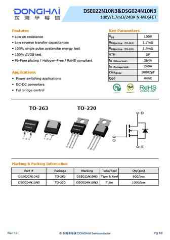
DSE022N10N3&DSG024N10N3 100V/1.7m /240A N-MOSFET Features Key Parameters VDS Low on resistance 100V RDS(on)typ. TO-263 Low reverse transfer capacitances 1.7m RDS(on)typ. TO-220 100% single pulse avalanche energy test 1.9m 100% VDS test VTH 3V ID Silicon limit Pb-Free plating / Halogen-Free / RoHS compliant 364A ID Package limit 240A
dse026n10na dsg028n10na.pdf
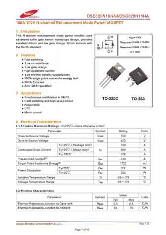
DSE026N10NA&DSG028N10NA 180A 100V N-channel Enhancement Mode Power MOSFET 1 Description This N-channel enhancement mode power mosfets used 2 D V = 100V DSS advanced splite gate trench technology design, provided R = 2.4m T0-220 DS(on) (TYP) excellent Rdson and low gate charge. Which accords with G the RoHS standard. R = 2.2m T0-263 DS(on) (TYP) 1 3 S I = 180A D 2
Otros transistores... DHS046N10E, DHS046N10F, DHS046N10I, DHS051N10P, DHS052N10, DHS052N10B, DSE026N10N3A, DSE026N10NA, IRFZ24N, DSE043N14N, DSE047N08N3, DSE050N14N, DSE051N08N3, DSE054N10N3, DSE058N15NA, DSE065N10L3A, DSE108N20NA
History: SI4636DY
🌐 : EN ES РУ

Liste
Recientemente añadidas las descripciónes de los transistores:
MOSFET: BCD70N07A | BCD90N03 | BCD80N06 | T50N06 | H50N06 | BCD12N65 | BCT12N65 | BCD4N65 | BCT4N65 | BCD7N65 | BCT7N65 | BCT20N65 | ASDM30P100KQ | ASDM30N90Q | ASDM30N75KQ | ASDM30N150Q
Popular searches
irfp250n datasheet | 2n5550 | 2sd1047 | 2n3035 | ksc1815 | bu406 | j201 datasheet | 2n5088 datasheet