DSE028N10N3 Datasheet. Specs and Replacement
Type Designator: DSE028N10N3 📄📄
Type of Transistor: MOSFET
Type of Control Channel: N-Channel
Absolute Maximum Ratings
Pd ⓘ - Maximum Power Dissipation: 312 W
|Vds|ⓘ - Maximum Drain-Source Voltage: 100 V
|Vgs|ⓘ - Maximum Gate-Source Voltage: 20 V
|Id| ⓘ - Maximum Drain Current: 170 A
Tj ⓘ - Maximum Junction Temperature: 150 °C
Electrical Characteristics
tr ⓘ - Rise Time: 105 nS
Cossⓘ - Output Capacitance: 2710 pF
RDSonⓘ - Maximum Drain-Source On-State Resistance: 0.0028 Ohm
Package: TO263
📄📄 Copy
DSE028N10N3 substitution
- MOSFET ⓘ Cross-Reference Search
DSE028N10N3 datasheet
dsg030n10n3 dse028n10n3.pdf
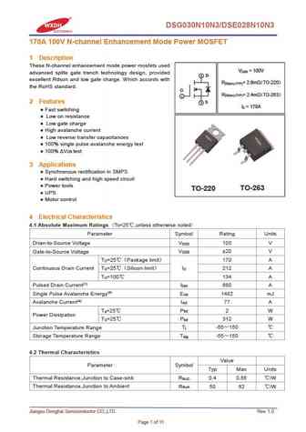
DSG030N10N3/DSE028N10N3 170A 100V N-channel Enhancement Mode Power MOSFET 1 Description These N-channel enhancement mode power mosfets used V = 100V DSS advanced splite gate trench technology design, provided 2 D excellent Rdson and low gate charge. Which accords with R = 2.6m TO-220 DS(on) (TYP) the RoHS standard. G R = 2.4m TO-263 DS(on) (TYP) 1 2 Features 3 ... See More ⇒
dse026n10n3a.pdf
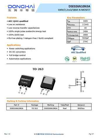
DSE026N10N3A 100V/2.2m /180A N-MOSFET Features Key Parameters VDS AEC-Q101 qualified 100V RDS(on)typ. Low on resistance 2.2m Low reverse transfer capacitances VTH 3V ID(Silicon limit) 100% single pulse avalanche energy test 240A ID (Package limit) 100% VDS test 180A Ciss@10V Pb-Free plating / Halogen-Free / RoHS compliant 7035pF Qgd 27nC Application... See More ⇒
dse022n10n3 dsg024n10n3.pdf
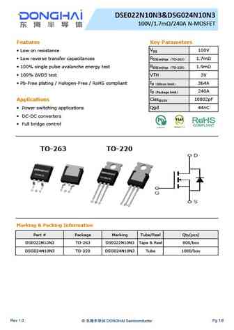
DSE022N10N3&DSG024N10N3 100V/1.7m /240A N-MOSFET Features Key Parameters VDS Low on resistance 100V RDS(on)typ. TO-263 Low reverse transfer capacitances 1.7m RDS(on)typ. TO-220 100% single pulse avalanche energy test 1.9m 100% VDS test VTH 3V ID Silicon limit Pb-Free plating / Halogen-Free / RoHS compliant 364A ID Package limit 240A ... See More ⇒
dse026n10na dsg028n10na.pdf
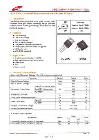
DSE026N10NA&DSG028N10NA 180A 100V N-channel Enhancement Mode Power MOSFET 1 Description This N-channel enhancement mode power mosfets used 2 D V = 100V DSS advanced splite gate trench technology design, provided R = 2.4m T0-220 DS(on) (TYP) excellent Rdson and low gate charge. Which accords with G the RoHS standard. R = 2.2m T0-263 DS(on) (TYP) 1 3 S I = 180A D 2... See More ⇒
Detailed specifications: DHS046N10E, DHS046N10F, DHS046N10I, DHS051N10P, DHS052N10, DHS052N10B, DSE026N10N3A, DSE026N10NA, IRFZ24N, DSE043N14N, DSE047N08N3, DSE050N14N, DSE051N08N3, DSE054N10N3, DSE058N15NA, DSE065N10L3A, DSE108N20NA
Keywords - DSE028N10N3 MOSFET specs
DSE028N10N3 cross reference
DSE028N10N3 equivalent finder
DSE028N10N3 pdf lookup
DSE028N10N3 substitution
DSE028N10N3 replacement
Need a MOSFET replacement? Our guide shows you how to find a perfect substitute by comparing key parameters and specs
