NVMFS4841N MOSFET Equivalente. Reemplazo. Hoja de especificaciones. Principales características
Número de Parte: NVMFS4841N
Tipo de FET: MOSFET
Polaridad de transistor: N
ESPECIFICACIONES MÁXIMAS
Pdⓘ - Máxima disipación de potencia: 3.7 W
|Vds|ⓘ - Voltaje máximo drenador-fuente: 30 V
|Vgs|ⓘ - Voltaje máximo fuente-puerta: 20 V
|Id|ⓘ - Corriente continua de drenaje: 16 A
Tjⓘ - Temperatura máxima de unión: 175 °C
CARACTERÍSTICAS ELÉCTRICAS
trⓘ - Tiempo de subida: 66.5 nS
Cossⓘ - Capacitancia de salida: 348 pF
RDSonⓘ - Resistencia estado encendido drenaje a fuente: 0.007 Ohm
Encapsulados: SO8FL
Búsqueda de reemplazo de NVMFS4841N MOSFET
- Selecciónⓘ de transistores por parámetros
NVMFS4841N datasheet
nvmfs4841n.pdf
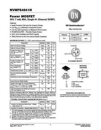
NVMFS4841N Power MOSFET 30V, 7 mW, 89A, Single N-Channel SO8FL Features Small Footprint (5x6 mm) for Compact Design Low RDS(on) to Minimize Conduction Losses http //onsemi.com Low QG and Capacitance to Minimize Driver Losses NVMFS4841NWF - Wettable Flanks Product AEC-Q101 Qualified and PPAP Capable V(BR)DSS RDS(ON) MAX ID MAX These Devices are Pb-Free and are
nvmfs4841n-d.pdf
NVMFS4841N Power MOSFET 30V, 7 mW, 89A, Single N-Channel SO8FL Features Small Footprint (5x6 mm) for Compact Design Low RDS(on) to Minimize Conduction Losses http //onsemi.com Low QG and Capacitance to Minimize Driver Losses AEC-Q101 Qualified These are Pb-Free Devices* V(BR)DSS RDS(ON) MAX ID MAX 7.0 mW @ 10 V MAXIMUM RATINGS (TJ = 25 C unless otherwise noted)
nvmfs4c302n.pdf
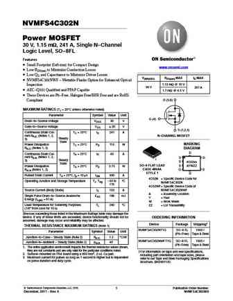
NVMFS4C302N Power MOSFET 30 V, 1.15 mW, 241 A, Single N-Channel Logic Level, SO-8FL Features Small Footprint (5x6 mm) for Compact Design www.onsemi.com Low RDS(on) to Minimize Conduction Losses Low QG and Capacitance to Minimize Driver Losses V(BR)DSS RDS(on) MAX ID MAX NVMFS4C302NWF - Wettable Flanks Option for Enhanced Optical 1.15 mW @ 10 V Inspection 30 V 241 A
nvmfs4c05n.pdf
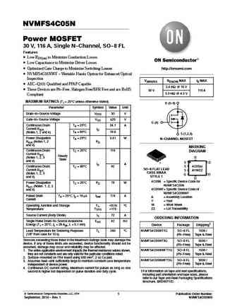
NVMFS4C05N Power MOSFET 30 V, 116 A, Single N-Channel, SO-8 FL Features Low RDS(on) to Minimize Conduction Losses Low Capacitance to Minimize Driver Losses Optimized Gate Charge to Minimize Switching Losses http //onsemi.com NVMFS4C05NWF - Wettable Flanks Option for Enhanced Optical Inspection V(BR)DSS RDS(ON) MAX ID MAX AEC-Q101 Qualified and PPAP Capable 3.4 mW
Otros transistores... NUS5531MT , NVD5803N , NVD5862N , NVD5863NL , NVD5865NL , NVD5867NL , NVD5890N , NVMFD5877NL , IRFZ46N , NVTFS4823N , NVTFS4824N , NVTFS5116PL , NVTFS5811NL , NVTFS5820NL , NVTFS5826NL , SCH1330 , SCH1331 .
🌐 : EN ES РУ

Liste
Recientemente añadidas las descripciónes de los transistores:
MOSFET: AUB062N08BG | AUB060N08AG | AUB056N10 | AUB056N08BGL | AUB050N085 | AUB050N055 | AUB045N12 | AUB045N10BT | AUB039N10 | AUB034N10 | AUB033N08BG | AUB026N085 | AUA062N08BG | AUA060N08AG | AUA056N08BGL | AUA039N10
Popular searches
2n7000 equivalent | tip31 | tip122 transistor | 2sc1079 | 2sc1815 equivalent | 2sa1220 | 2sa940 | 2sc627