C100 Equivalente. Reemplazo. Hoja de especificaciones. Principales características
Número de Parte: C100
Material: Si
Polaridad de transistor: PNP
ESPECIFICACIONES MÁXIMAS
Disipación total del dispositivo (Pc): 0.75 W
Tensión colector-base (Vcb): 60 V
Tensión colector-emisor (Vce): 50 V
Corriente del colector DC máxima (Ic): 1 A
Temperatura operativa máxima (Tj): 175 °C
CARACTERÍSTICAS ELÉCTRICAS
Ganancia de corriente contínua (hFE): 50
Encapsulados: TO106
Búsqueda de reemplazo de C100
- Selecciónⓘ de transistores por parámetros
C100 datasheet
c100 d100.pdf
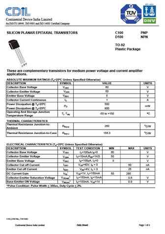
Continental Device India Limited An ISO/TS 16949, ISO 9001 and ISO 14001 Certified Company SILICON PLANAR EPITAXIAL TRANSISTORS C100 PNP D100 NPN TO-92 Plastic Package E CB These are complementary transistors for medium power voltage and current amplifier applications. ABSOLUTE MAXIMUM RATINGS (Ta=25 C Unless Specified Otherwise) DESCRIPTION SYMBOL VALUE UNITS VCBO Collector Base
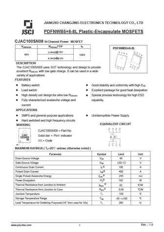
cjac100sn08u.pdf
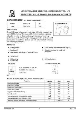
JIANGSU CHANGJING ELECTRONICS TECHNOLOGY CO., LTD PDFN 5 6-8L-B Plastic-Encapsulate MOSFETS CJAC100SN08U N-Channel Power MOSFET ID V(BR)DSS RDS(on)TYP PDFN 5 6-8L-B 80 V 100A 3.0m @10V DESCRIPTION These N-Channel enhancement mode power field effect transistors are using SGT technology.This advanced technology has been especially tailored to minimize on-state resistance, pr
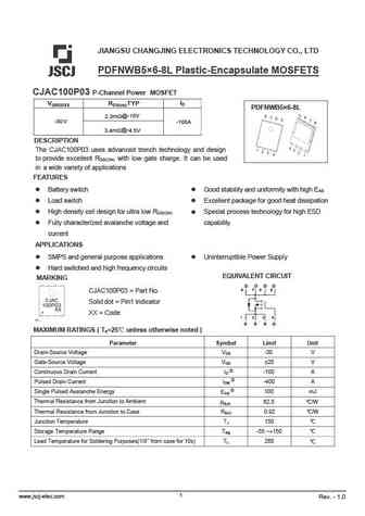
cjac100p03.pdf
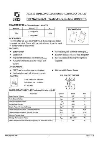
JIANGSU CHANGJING ELECTRONICS TECHNOLOGY CO., LTD PDFN 5 6-8L Plastic-Encapsulate MOSFETS CJAC100P03 P-Channel Power MOSFET ID V(BR)DSS RDS(on)TYP PDFN 5 6-8L 2.3m @-10V -30 V -100A 3.4m @-4.5V DESCRIPTION The CJAC100P03 uses advanced trench technology and design to provide excellent RDS(ON) with low gate charge. It can be used in a wide variety of applications FEATU
irgc100b120k.pdf
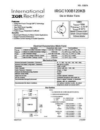
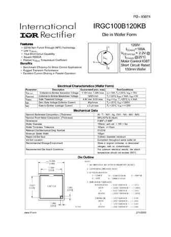
PD - 93874 IRGC100B120KB Die in Wafer Form Features Features Features Features Features 1200V C GEN5 Non Punch Through (NPT) Technology IC(nom)= 100A Low VCE(on) VCE(on) typ.= 2.2V @ 10 s Short Circuit Capability Square RBSOA IC(nom) @ 25 C Positive VCE(on) Temperature Coefficient Motor Control IGBT G Benefits Short Circuit Rated Benchmark E
irgc100b60kb.pdf
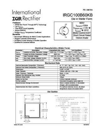
PD - 94618A IRGC100B60KB Die in Wafer Form Features 600V C GEN5 Non Punch Through (NPT) Technology IC(nom)=100A Low VCE(on) VCE(on) typ.=1.9V @ 10 s Short Circuit Capability Square RBSOA IC(nom) @ 25 C Positive VCE(on) Temperature Coefficient Motor Control IGBT G Benefits Short Circuit Rated Benchmark Efficiency for Motor Control Applications E
irgc100b60ub.pdf
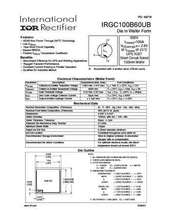
PD - 94716 IRGC100B60UB Die in Wafer Form Features 600V C GEN5 Non Punch Through (NPT) Technology IC(nom)=100A Low VCE(on) VCE(on) typ. = 2.8V 10 s Short Circuit Capability Square RBSOA @ IC(nom) @ 25 C Positive VCE(on) Temperature Coefficient UPS IGBT G Benefits Short Circuit Rated Benchmark Efficiency for UPS and Welding Applications E 150mm Waf
irgc100b120ub.pdf
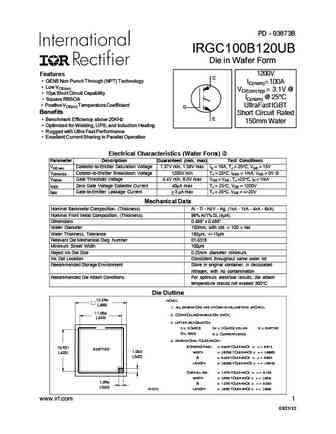
PD - 93873B IRGC100B120UB Die in Wafer Form 1200V Features C GEN5 Non Punch Through (NPT) Technology IC(nom)= 100A Low VCE(on) VCE(on) typ.= 3.1V @ 10 s Short Circuit Capability IC(nom) @ 25 C Square RBSOA Positive VCE(on) Temperature Coefficient UltraFast IGBT G Benefits Short Circuit Rated E Benchmark Efficiency above 20KHz 150mm Wafer
irgc100b120u.pdf

PD - 93873 IRGC100B120UB Die in Wafer Form Features Features Features Features Features 1200V C GEN5 Non Punch Through (NPT) Technology IC(nom)= 100A Low VCE(on) VCE(on) typ.= 3.1V @ 10 s Short Circuit Capability Square RBSOA IC(nom) @ 25 C Positive VCE(on) Temperature Coefficient UltraFast IGBT G Benefits Short Circuit Rated Benchmark Effic
msc1004mp.pdf
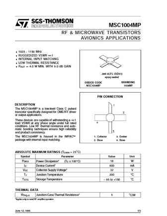
MSC1004MP RF & MICROWAVE TRANSISTORS AVIONICS APPLICATIONS .1025 - 1150 MHz .RUGGEDIZED VSWR 1 .INTERNAL INPUT MATCHING .LOW THERMAL RESISTANCE .P 4.0 W MIN. WITH 9.0 dB GAIN OUT = .280 4LFL (SO51) epoxy sealed ORDER CODE BRANDING MSC1004MP 1004MP PIN CONNECTION DESCRIPTION The MSC1004MP is a low-level Class C pulsed transistor specifically designed for DME/IFF driver or ou
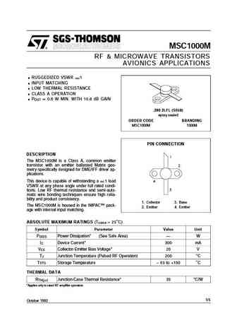
msc1000m.pdf

MSC1000MP RF & MICROWAVE TRANSISTORS AVIONICS APPLICATIONS .RUGGEDIZED VSWR 1 .INPUT MATCHING .LOW THERMAL RESISTANCE .CLASS A OPERATION .P 0.6 W MIN. WITH 10.8 dB GAIN OUT = .280 4LSL (S053) epoxy sealed ORDER CODE BRANDING MSC1000MP 1000MP PIN CONNECTION DESCRIPTION The MSC1000MP is a Class A, common emitter transistor with an emitter ballasted Matrix geo- metry specifi
msc1000.pdf
MSC1000M RF & MICROWAVE TRANSISTORS AVIONICS APPLICATIONS .RUGGEDIZED VSWR 1 .INPUT MATCHING .LOW THERMAL RESISTANCE .CLASS A OPERATION .P 0.6 W MIN. WITH 10.8 dB GAIN OUT = .280 2LFL (S058) epoxy sealed ORDER CODE BRANDING MSC1000M 1000M PIN CONNECTION DESCRIPTION The MSC1000M is a Class A, common emitter transistor with an emitter ballasted Matrix geo- metry specificall
msc1004m.pdf
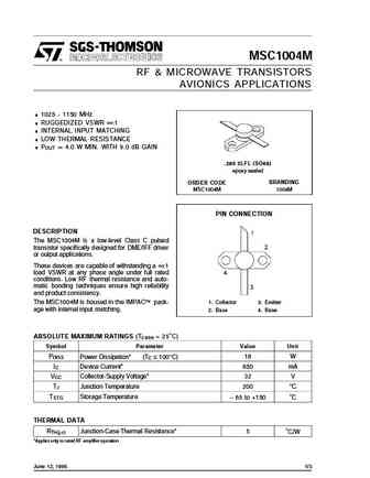
MSC1004M RF & MICROWAVE TRANSISTORS AVIONICS APPLICATIONS .1025 - 1150 MHz .RUGGEDIZED VSWR 1 .INTERNAL INPUT MATCHING .LOW THERMAL RESISTANCE .P 4.0 W MIN. WITH 9.0 dB GAIN OUT = .280 2LFL (SO68) epoxy sealed ORDER CODE BRANDING MSC1004M 1004M PIN CONNECTION DESCRIPTION The MSC1004M is a low-level Class C pulsed transistor specifically designed for DME/IFF driver or output
ksc1008.pdf
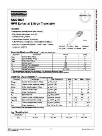
September 2006 KSC1008 tm NPN Epitacial Silicon Transistor Features Low frequency amplifier medium speed switching. High Collector-Base Voltage VCBO=80V. Collector Current IC=700mA Collector Power Dissipation PC=800mW TO-92 Suffix -C means Center Collector (1.Emitter 2.Collector 3.Base) Non suffix -C means Side Collector (1.Emitter 2.Base 3.C
ksc1009.pdf
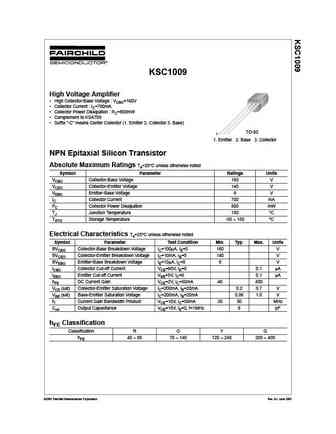
KSC1009 High Voltage Amplifier High Collector-Base Voltage VCBO=160V Collector Current IC=700mA Collector Power Dissipation PC=800mW Complement to KSA709 Suffix -C means Center Collector (1. Emitter 2. Collector 3. Base) TO-92 1 1. Emitter 2. Base 3. Collector NPN Epitaxial Silicon Transistor Absolute Maximum Ratings Ta=25 C unless otherwise noted S
rf4c100bc.pdf
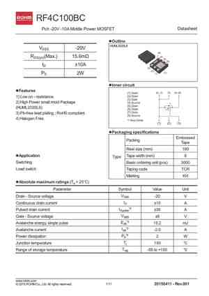
RF4C100BC Datasheet Pch -20V -10A Middle Power MOSFET lOutline l HUML2020L8 VDSS -20V RDS(on)(Max.) 15.6m ID 10A PD 2W lInner circuit l lFeatures l 1) Low on - resistance. 2) High Power small mold Package (HUML2020L8). 3) Pb-free lead plating ; RoHS compliant. 4) Halog
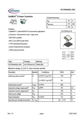
ipc100n04s5-1r2.pdf
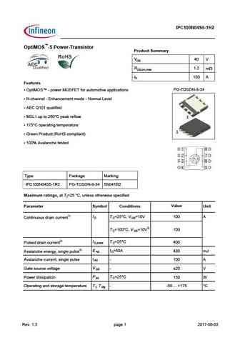
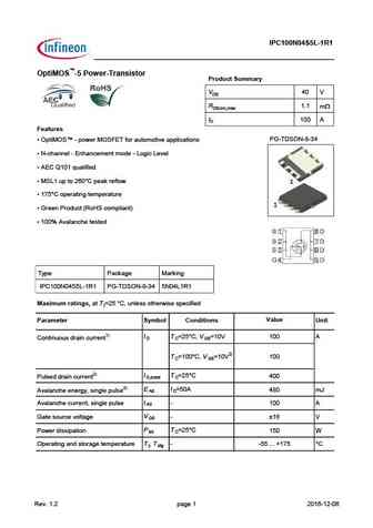
IPC100N04S5-1R2 OptiMOS -5 Power-Transistor Product Summary VDS 40 V RDS(on),max 1.2 mW ID 100 A Features PG-TDSON-8-34 OptiMOS - power MOSFET for automotive applications N-channel - Enhancement mode - Normal Level AEC Q101 qualified MSL1 up to 260 C peak reflow 1 175 C operating temperature 1 Green Product (RoHS compliant) 100% Avalan
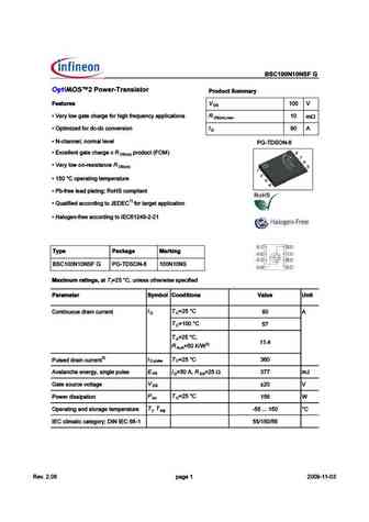
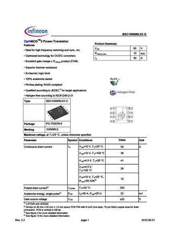
bsc100n06ls3g.pdf
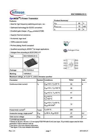
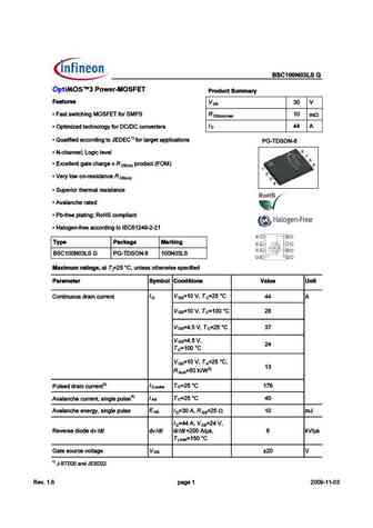
Type BSC100N06LS3 G OptiMOSTM3 Power-Transistor Product Summary Features VDS 60 V Ideal for high frequency switching and sync. rec. RDS(on),max 10 mW Optimized technology for DC/DC converters ID 50 A Excellent gate charge x R product (FOM) DS(on) Superior thermal resistance N-channel, logic level 100% avalanche tested Pb-free plating; RoHS compli
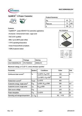
iauc100n04s6n015.pdf

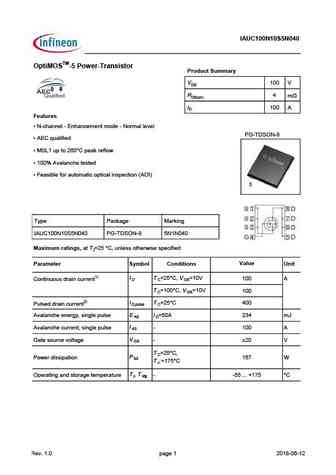
IAUC100N04S6N015 OptiMOS - 6 Power-Transistor Product Summary VDS 40 V RDS(on),max 1.5 mW ID 100 A Features PG-TDSON-8 OptiMOS - power MOSFET for automotive applications N-channel - Enhancement mode - Normal Level AEC Q101 qualified MSL1 up to 260 C peak reflow 1 175 C operating temperature 1 Green Product (RoHS compliant) 100% Avalanche teste
sigc100t65r3e.pdf
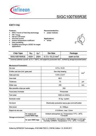
SIGC100T65R3E IGBT3 Chip Features Recommended for 650V Trench & Field Stop technology power modules low VCE(sat) C low turn-off losses Applications short tail current drives positive temperature coefficient easy paralleling G E Qualified according to JEDEC for target applications Chip Type VCE ICn1 ) Die Size Package SIGC100T65R
iauc100n04s6l020.pdf

IAUC100N04S6L020 OptiMOS - 6 Power-Transistor Product Summary VDS 40 V RDS(on),max 2.0 mW ID 100 A Features PG-TDSON-8 OptiMOS - power MOSFET for automotive applications N-channel - Enhancement mode - Logic Level AEC Q101 qualified MSL1 up to 260 C peak reflow 1 175 C operating temperature 1 Green Product (RoHS compliant) 100% Avalanche tested
ipc100n04s5l-2r6.pdf
IPC100N04S5L-2R6 OptiMOS -5 Power-Transistor Product Summary VDS 40 V RDS(on),max 2.6 mW ID 100 A Features PG-TDSON-8-33 OptiMOS - power MOSFET for automotive applications N-channel - Enhancement mode - Logic Level AEC Q101 qualified MSL1 up to 260 C peak reflow 1 175 C operating temperature 1 Green Product (RoHS compliant) 100% Avalanc
ipc100n04s5-1r9.pdf

IPC100N04S5-1R9 OptiMOS -5 Power-Transistor Product Summary VDS 40 V RDS(on),max 1.9 mW ID 100 A Features PG-TDSON-8-34 OptiMOS - power MOSFET for automotive applications N-channel - Enhancement mode - Normal Level AEC Q101 qualified MSL1 up to 260 C peak reflow 1 175 C operating temperature 1 Green Product (RoHS compliant) 100% Avalan
iauc100n08s5n043.pdf
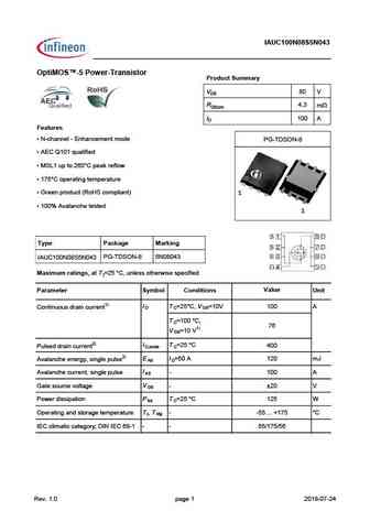
IAUC100N08S5N043 OptiMOS -5 Power-Transistor Product Summary VDS 80 V RDS(on) 4.3 mW ID 100 A Features N-channel - Enhancement mode PG-TDSON-8 AEC Q101 qualified MSL1 up to 260 C peak reflow 175 C operating temperature Green product (RoHS compliant) 1 100% Avalanche tested 1 Type Package Marking PG-TDSON-8 5N08043 IAUC100N08S5N043 Maximum ratings,
bsc100n03msg.pdf
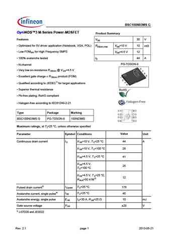
BSC100N03MS G OptiMOS 3 M-Series Power-MOSFET Product Summary Features VDS 30 V Optimized for 5V driver application (Notebook, VGA, POL) RDS(on),max VGS=10 V 10 mW Low FOMSW for High Frequency SMPS VGS=4.5 V 12 100% avalanche tested ID 44 A PG-TDSON-8 N-channel Very low on-resistance R @ V =4.5 V DS(on) GS Excellent gate charge x R product (FOM) DS
iauc100n04s6l014.pdf
IAUC100N04S6L014 OptiMOS - 6 Power-Transistor Product Summary VDS 40 V RDS(on),max 1.4 mW ID 100 A Features PG-TDSON-8 OptiMOS - power MOSFET for automotive applications N-channel - Enhancement mode - Logic Level AEC Q101 qualified MSL1 up to 260 C peak reflow 1 175 C operating temperature 1 Green Product (RoHS compliant) 100% Avalanche tested
ipc100n04s5-2r8.pdf

IPC100N04S5-2R8 OptiMOS -5 Power-Transistor Product Summary VDS 40 V RDS(on),max 2.8 mW ID 100 A Features PG-TDSON-8-33 OptiMOS - power MOSFET for automotive applications N-channel - Enhancement mode - Normal Level AEC Q101 qualified MSL1 up to 260 C peak reflow 1 175 C operating temperature 1 Green Product (RoHS compliant) 100% Avalanc
iauc100n04s6n028.pdf

IAUC100N04S6N028 OptiMOS - 6 Power-Transistor Product Summary VDS 40 V RDS(on),max 2.8 mW ID 100 A Features PG-TDSON-8 OptiMOS - power MOSFET for automotive applications N-channel - Enhancement mode - Normal Level AEC Q101 qualified MSL1 up to 260 C peak reflow 1 175 C operating temperature 1 Green Product (RoHS compliant) 100% Avalanche teste
bsc100n03ms.pdf

BSC100N03MS G OptiMOS 3 M-Series Power-MOSFET Product Summary Features VDS 30 V Optimized for 5V driver application (Notebook, VGA, POL) RDS(on),max VGS=10 V 10 mW Low FOMSW for High Frequency SMPS VGS=4.5 V 12 100% avalanche tested ID 44 A PG-TDSON-8 N-channel Very low on-resistance R @ V =4.5 V DS(on) GS Excellent gate charge x R product (FOM) DS
sigc100t60r3.pdf

SIGC100T60R3E IGBT3 Chip Features This chip is used for 600V Trench & Field Stop technology power module C low VCE(sat) low turn-off losses Applications short tail current drives positive temperature coefficient G easy paralleling E Chip Type VCE IC Die Size Package SIGC100T60R3E 600V 200A 9.73 x 10.23 mm2 sawn on foil Mechanical Par
iauc100n04s6n022.pdf
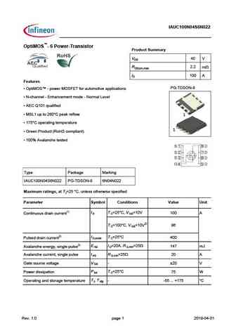
IAUC100N04S6N022 OptiMOS - 6 Power-Transistor Product Summary VDS 40 V RDS(on),max 2.2 mW ID 100 A Features PG-TDSON-8 OptiMOS - power MOSFET for automotive applications N-channel - Enhancement mode - Normal Level AEC Q101 qualified MSL1 up to 260 C peak reflow 1 175 C operating temperature 1 Green Product (RoHS compliant) 100% Avalanche teste
ipc100n04s5l-1r1.pdf
IPC100N04S5L-1R1 OptiMOS -5 Power-Transistor Product Summary VDS 40 V RDS(on),max 1.1 mW ID 100 A Features PG-TDSON-8-34 OptiMOS - power MOSFET for automotive applications N-channel - Enhancement mode - Logic Level AEC Q101 qualified MSL1 up to 260 C peak reflow 1 175 C operating temperature 1 Green Product (RoHS compliant) 100% Avalan
iauc100n04s6l025.pdf

IAUC100N04S6L025 OptiMOS - 6 Power-Transistor Product Summary VDS 40 V RDS(on),max 2.5 mW ID 100 A Features PG-TDSON-8 OptiMOS - power MOSFET for automotive applications N-channel - Enhancement mode - Logic Level AEC Q101 qualified MSL1 up to 260 C peak reflow 1 175 C operating temperature 1 Green Product (RoHS compliant) 100% Avalanche tested
igc100t65t8rm.pdf
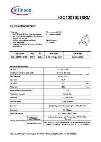
IGC100T65T8RM IGBT3 Chip Medium Power Features Recommended for 650V Trench & Field Stop technology power modules C high short circuit capability, self limiting short circuit current positive temperature coefficient Applications easy paralleling drives G Qualified according to JEDEC for target E applications Chip Type VCE ICn Die Size Package IGC100T6
bsc100n03ls.pdf
& " & E $;B1= !#& ' $=;0@/? &@99-=D Features D Q 2CD CG D49 ?8 ') - . 7@B -'*- 1 m D n) m x 44 Q ) AD > J65 D649?@=@8I 7@B 4@?F6BD6BC D 1) Q + E2= 7 65 244@B5 ?8 D@ $ 7@B D2B86D 2AA= 42D @?C G D ON Q ( 492??6= &@8 4 =6F6= Q H46==6?D 82D6 492B86 H AB@5E4D ) ' D n) Q /6BI =@G @? B6C CD2?46 D n) Q -EA6B @B D96B>2= B6C CD2?46 Q F2=2?496 B2D65 Q *3 7B66 A=2D ?8
bsc100n06ls3.pdf
pe % ! % TM # A0A= 2?E 1) R + F2= 7 65 244@C5 ?8 E@ $ 7@C E2C86E 2AA= 42E @?D R
iauc100n10s5l040.pdf
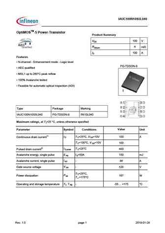
IAUC100N10S5L040 OptiMOSTM-5 Power-Transistor Product Summary VDS 100 V RDS(on) 4 mW ID 100 A Features N-channel - Enhancement mode - Logic level PG-TDSON-8 AEC qualified MSL1 up to 260 C peak reflow 100% Avalanche tested Feasible for automatic optical inspection (AOI) 1 Type Package Marking IAUC100N10S5L040 PG-TDSON-8 5N10L040 Maximum ratings, at T =25 C
sigc100t60r3e.pdf
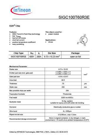
SIGC100T60R3E IGBT3 Chip Features This chip is used for 600V Trench & Field Stop technology power module C low VCE(sat) low turn-off losses Applications short tail current drives positive temperature coefficient G easy paralleling E Chip Type VCE IC Die Size Package SIGC100T60R3E 600V 200A 9.73 x 10.23 mm2 sawn on foil Mechanical Par
ipc100n04s5l-1r9.pdf

IPC100N04S5L-1R9 OptiMOS -5 Power-Transistor Product Summary VDS 40 V RDS(on),max 1.9 mW ID 100 A Features PG-TDSON-8-34 OptiMOS - power MOSFET for automotive applications N-channel - Enhancement mode - Logic Level AEC Q101 qualified MSL1 up to 260 C peak reflow 1 175 C operating temperature 1 Green Product (RoHS compliant) 100% Avalan
ipc100n04s5l-1r5.pdf

IPC100N04S5L-1R5 OptiMOS -5 Power-Transistor Product Summary VDS 40 V RDS(on),max 1.5 mW ID 100 A Features PG-TDSON-8-34 OptiMOS - power MOSFET for automotive applications N-channel - Enhancement mode - Logic Level AEC Q101 qualified MSL1 up to 260 C peak reflow 1 175 C operating temperature 1 Green Product (RoHS compliant) 100% Avalan
ixuc100n055.pdf
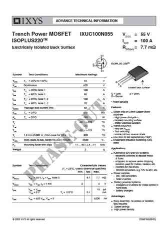
ADVANCE TECHNICAL INFORMATION Trench Power MOSFET IXUC100N055 VDSS = 55 V ISOPLUS220TM ID25 = 100 A Electrically Isolated Back Surface RDS(on)= 7.7 m ISOPLUS 220TM Symbol Test Conditions Maximum Ratings VDSS TJ = 25 C to 150 C55 V G D VGS Continuous 20 V S Isolated back surface* ID25 TC = 25 C; Note 1 100 A G = Gate, D = Drain, ID90 TC = 90 C, Note 1 8
ksc1008.pdf

ON Semiconductor Is Now To learn more about onsemi , please visit our website at www.onsemi.com onsemi and and other names, marks, and brands are registered and/or common law trademarks of Semiconductor Components Industries, LLC dba onsemi or its affiliates and/or subsidiaries in the United States and/or other countries. onsemi owns the rights to a number of patents, trademarks,
mc100el1648.pdf
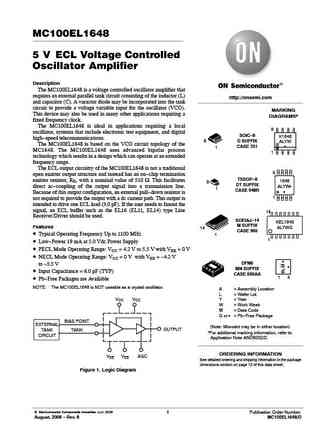
MC100EL1648 5 V ECL Voltage Controlled Oscillator Amplifier Description The MC100EL1648 is a voltage controlled oscillator amplifier that requires an external parallel tank circuit consisting of the inductor (L) http //onsemi.com and capacitor (C). A varactor diode may be incorporated into the tank circuit to provide a voltage variable input for the oscillator (VCO). MARKING This devi
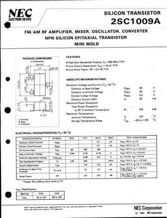
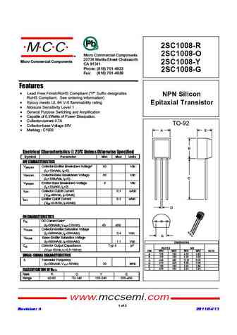
2sc1008.pdf
2SC1008 0.7A , 80 V NPN Plastic Encapsulated Transistor Elektronische Bauelemente RoHS Compliant Product A suffix of -C specifies halogen & lead-free TO-92 FEATURES General Purpose Switching and Amplification. G H Emitter Base Collector J CLASSIFICATION OF hFE A D Millimeter REF. Min. Max. Product-Rank 2SC1008-R 2SC1008-Q 2SC1008-Y 2SC1008-G B A
inc1001ac1.pdf
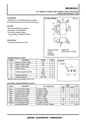
INC1001AC1 FOR GENERAL PURPOSE HIGH CURRENT DRIVE APPLICATION SILICON NPN EPITAXIAL TYPE DESCRIPTION OUTLINE DRAWING UNIT mm 2.8 INC1001AC1 is a silicon NPN epitaxial type transistor. 0.65 1.5 0.65 It is designed with high collector current and small VCE(sat). FEATURE Super mini package for easy mounting High collector current(IC=500mA) Low coll
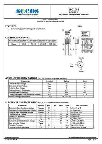
csc1008 csa708.pdf
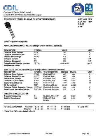
Continental Device India Limited An ISO/TS 16949, ISO 9001 and ISO 14001 Certified Company NPN/PNP EPITAXIAL PLANAR SILICON TRANSISTORS CSC1008 NPN CSA708 PNP TO-92 CBE Low Frequency Amplifier. ABSOLUTE MAXIMUM RATINGS(Ta=25deg C unless otherwise specified) DESCRIPTION SYMBOL VALUE UNIT Collector -Base Voltage VCBO 80 V Collector -Emitter Voltage VCEO 60 V Emitter -Base Voltage VEBO
csa709 csc1009.pdf
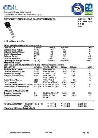
Continental Device India Limited An ISO/TS 16949, ISO 9001 and ISO 14001 Certified Company PNP/NPN EPITAXIAL PLANAR SILICON TRANSISTORS CSA709 PNP CSC1009 NPN TO-92 CBE High Voltage Amplifier. ABSOLUTE MAXIMUM RATINGS(Ta=25deg C ) DESCRIPTION SYMBOL CSA709 CSC1009 UNIT Collector -Base Voltage VCBO 160 160 V Collector -Emitter Voltage VCEO 150 140 V Emitter -Base Voltage VEBO 8.0 8.0
2sc1008.pdf
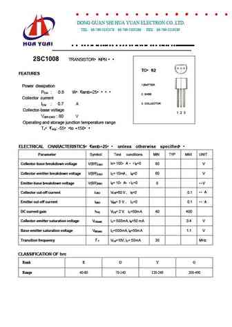
DONG GUAN SHI HUA YUAN ELECTRON CO.,LTD. TEL 86-769-5335378 86-769-5305266 FEX 86-769-5316189 TO-92 Plastic-Encapsulate Transistors 2SC1008 TRANSISTOR NPN TO 92 FEATURES 1.EMITTER Power dissipation PCM 0.8 W Tamb=25 2. BASE Collector current 3. COLLECTOR ICM 0.7 A Collector-base voltage 1 2 3 V(BR)CBO
2sc1008.pdf
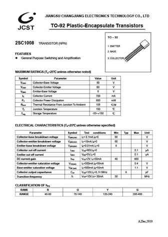
JIANGSU CHANGJIANG ELECTRONICS TECHNOLOGY CO., LTD TO-92 Plastic-Encapsulate Transistors TO 92 2SC1008 TRANSISTOR (NPN) 1. EMITTER 2. BASE FEATURES 3. COLLECTOR General Purpose Switching and Amplification MAXIMUM RATINGS (Ta=25 unless otherwise noted) Symbol Parameter Value Unit VCBO Collector-Base Voltage 80 V VCEO Collector-Emitter Voltage 60 V VEBO Emitter-
cjac100p03.pdf
JIANGSU CHANGJING ELECTRONICS TECHNOLOGY CO., LTD PDFN 5 6-8L Plastic-Encapsulate MOSFETS CJAC100P03 P-Channel Power MOSFET ID V(BR)DSS RDS(on)TYP PDFN 5 6-8L 2.3m @-10V -30 V -100A 3.4m @-4.5V DESCRIPTION The CJAC100P03 uses advanced trench technology and design to provide excellent RDS(ON) with low gate charge. It can be used in a wide variety of applications FEATU
cjac100sn08.pdf
JIANGSU CHANGJING ELECTRONICS TECHNOLOGY CO., LTD PDFN 5 6-8L Plastic-Encapsulate MOSFETS CJAC100SN08 N-Channel Power MOSFET ID V(BR)DSS RDS(on)TYP PDFN 5 6-8L 2.9m @10V 80V 100A 4.3m @4.5V DESCRIPTION The CJAC100SN08 uses SGT technology and design to provide excellent RDS(ON) with low gate charge. It can be used in a wide variety of applications FEATURES Batte
ktc1006.pdf
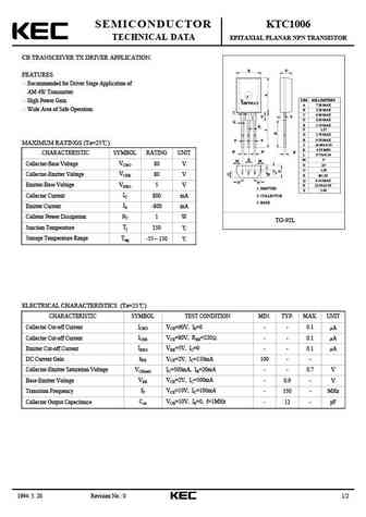
SEMICONDUCTOR KTC1006 TECHNICAL DATA EPITAXIAL PLANAR NPN TRANSISTOR CB TRANSCEIVER TX DRIVER APPLICATION. B D FEATURES Recommended for Driver Stage Application of AM 4W Transmitter. DIM MILLIMETERS P High Power Gain. DEPTH 0.2 A 7.20 MAX Wide Area of Safe Operation. B 5.20 MAX C C 0.60 MAX S D 2.50 MAX Q E 1.15 MAX K F 1.27 G 1.70 MAX H 0.55 MAX FF MAXIMUM RATINGS (T
ktc1003.pdf
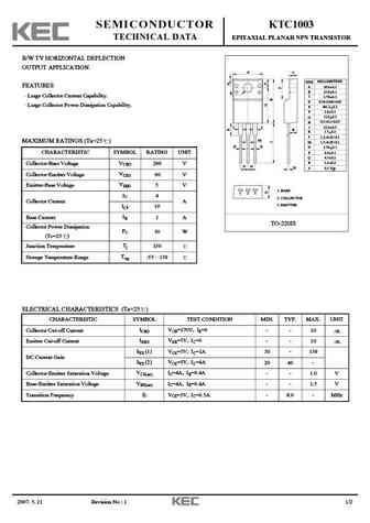
SEMICONDUCTOR KTC1003 TECHNICAL DATA EPITAXIAL PLANAR NPN TRANSISTOR B/W TV HORIZONTAL DEFLECTION OUTPUT APPLICATION. A C DIM MILLIMETERS S _ FEATURES A 10.0 + 0.3 _ + B 15.0 0.3 E Large Collector Current Capability. C _ 2.70 0.3 + D 0.76+0.09/-0.05 Large Collector Power Dissipation Capability. _ E 3.2 0.2 + _ F 3.0 0.3 + _ 12.0 0.3 G + H 0.5+0.1/-0.05 _ + J 1
ktc1008.pdf
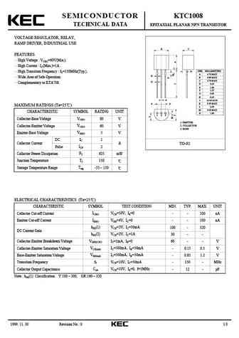
SEMICONDUCTOR KTC1008 TECHNICAL DATA EPITAXIAL PLANAR NPN TRANSISTOR VOLTAGE REGULATOR, RELAY, RAMP DRIVER, INDUSTRIAL USE B C FEATURES High Voltage VCEO=60V(Min.). High Current IC(Max.)=1A. N DIM MILLIMETERS High Transition Frequency fT=150MHz(Typ.). A 4.70 MAX E K B 4.80 MAX Wide Area of Safe Operation. G C 3.70 MAX D Complementary to KTA708. D 0.45 E 1.00 F 1
2sc1008.pdf
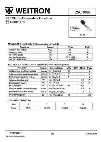
WEITRON 2SC1008 NPN Plastic-Encapsulate Transistor P b Lead(Pb)-Free 1. EMITTER 2. COLLECTOR 3. BASE TO-92 MAXIMUM RATINGS (T unless otherwise noted) A=25 C Parameter Symbol Value Units Collector-Base Voltage V VCBO 80 A Collector Current ICM 0.7 Power Dissipation PCM 0.8 W -55 to +150 Junction Temperature TJ C -55 to +150 Tstg Storage Temperature C ELECTRICAL CHARACTE
fhc100.pdf
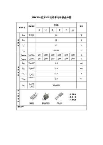
FHC100 PNP B C D E F G PCM Tc=25 100 W ICM 12 A Tjm 175 Tstg -55 150 V(BR)CBO ICB=2mA 50 100 150 200 250 300 V V(BR)CEO ICE=2mA 50 100 150 200 250 300 V ICBO VCB=20V 2.0 mA ICEO VCE=20V 2.0 mA VBEsat 2.5 V IC
ftc1008.pdf
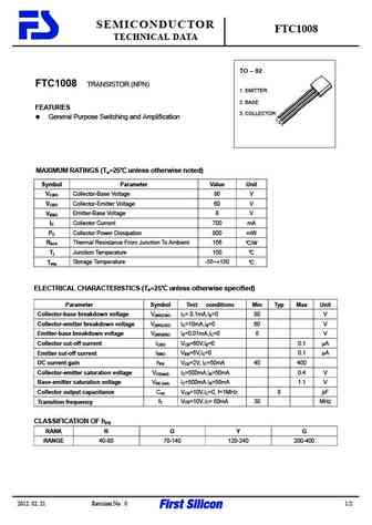
SEMICONDUCTOR FTC1008 TECHNICAL DATA TO 92 FTC1008 TRANSISTOR (NPN) 1. EMITTER 2. BASE FEATURES 3. COLLECTOR General Purpose Switching and Amplification MAXIMUM RATINGS (Ta=25 unless otherwise noted) Symbol Parameter Value Unit VCBO Collector-Base Voltage 80 V VCEO Collector-Emitter Voltage 60 V VEBO Emitter-Base Voltage 8 V IC Collector Current 700 mA PC Col
2sc1009.pdf
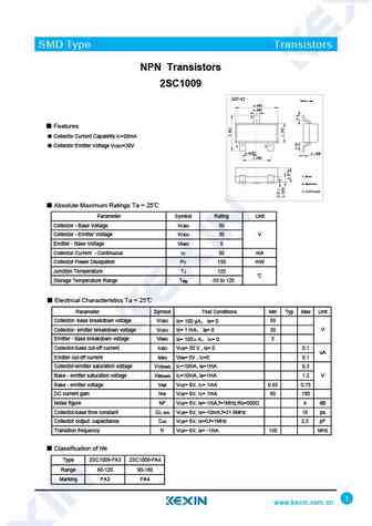
SMD Type Transistors NPN Transistors 2SC1009 SOT-23 Unit mm +0.1 2.9 -0.1 +0.1 0.4 -0.1 3 Features Collector Current Capability IC=50mA Collector Emitter Voltage VCEO=30V 1 2 +0.1 +0.05 0.95-0.1 0.1-0.01 +0.1 1.9-0.1 1.Base 2.Emitter 3.collector Absolute Maximum Ratings Ta = 25 Parameter Symbol Rating Unit Collector - Base Voltage VCBO 50 Collecto
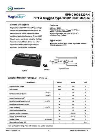
mpmc100b120rh.pdf
MPMC100B120RH NPT & Rugged Type 1200V IGBT Module General Description Features MagnaChip s IGBT Module 7DM-2 package BV = 1200V CES Low Conduction Loss V = 2.8V (typ.) CE(sat) devices are optimized to reduce losses and Fast & Soft Anti-Parallel FWD switching noise in high frequency power Short circuit rated Min. 10us at TC=100 Isolation Type
bcx70h bcx70j bcx70k bsr13 tmpc1009 tmpc1009 tmpc1009 tmpc1009 tmpc1009 tmpc1622 tmpc1622 tmpc1622 tmpc1623.pdf
2sc1008.pdf
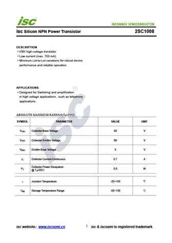
INCHANGE Semiconductor isc Silicon NPN Power Transistor 2SC1008 DESCRIPTION NPN high-voltage transistor Low current (max. 700 mA) Minimum Lot-to-Lot variations for robust device performance and reliable operation APPLICATIONS Designed for Switching and amplification in high voltage applications , such as telephony applications. ABSOLUTE MAXIMUM RATINGS(T =25 ) a SYMBOL PA
ktc1003.pdf
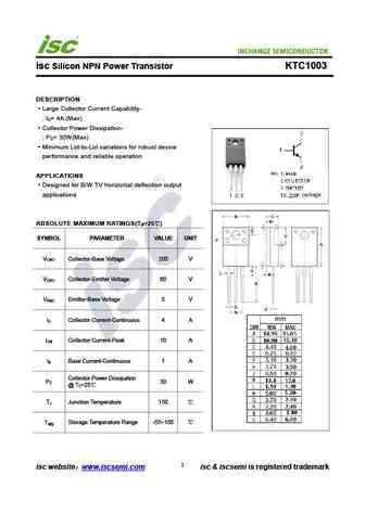
isc Silicon NPN Power Transistor KTC1003 DESCRIPTION Large Collector Current Capability- I = 4A (Max) C Collector Power Dissipation- P = 30W(Max) C Minimum Lot-to-Lot variations for robust device performance and reliable operation APPLICATIONS Designed for B/W TV horizontal deflection output applications ABSOLUTE MAXIMUM RATINGS(T =25 ) a SYMBOL PARAMETER VALUE UNIT
2sc1004.pdf
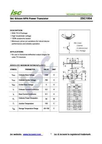
INCHANGE Semiconductor isc Silicon NPN Power Transistor 2SC1004 DESCRIPTION With TO-3 Package High breakdown voltage 100% avalanche tested Minimum Lot-to-Lot variations for robust device performance and reliable operation APPLICATIONS for use in horizontal deflection output stages for color TV receives ABSOLUTE MAXIMUM RATINGS(T =25 ) a SYMBOL PARAMETER VALUE UNIT V Co
Otros transistores... BUYP54 , BVW90 , BVX18A , C055 , C055P , C066 , C066P , C1 , S9013 , C1001 , C1002 , C1003 , C1004 , C101 , C102 , C103 , C106 .
🌐 : EN ES РУ

Liste
Recientemente añadidas las descripciónes de los transistores:
BJT: GA1A4M | SBT42 | 2SA200-Y | 2SA200-O | 2SD882-Q | 2SD882-P | 2SD882-E | 2SC945-L | 2SC945-H | 2SC4226-R23 | 2SC3357-F | 2SC3357-E | 2SC3356-R26 | 2SC3356-R24 | 2SC3356-R23 | 2SB772-Q | 2SB772-P | 2SB772-E | 2SA1015-L | 2SA1015-H | HSS8550
Popular searches
ac128 transistor | 2n3055 transistor | 2n3904 datasheet | irf3710 | tip3055 | mosfet datasheet | irf3205 datasheet | irf5210