D150 Datasheet. Equivalente. Reemplazo. Hoja de especificaciones. Principales características
Número de Parte: D150 📄📄
Material: Si
Polaridad de transistor: NPN
ESPECIFICACIONES MÁXIMAS
Disipación total del dispositivo (Pc): 0.5 W
Tensión colector-base (Vcb): 35 V
Tensión colector-emisor (Vce): 30 V
Tensión emisor-base (Veb): 1 V
Corriente del colector DC máxima (Ic): 1 A
Temperatura operativa máxima (Tj): 175 °C
CARACTERÍSTICAS ELÉCTRICAS
Transición de frecuencia (fT): 80 MHz
Ganancia de corriente contínua (hFE): 50
Encapsulados: TO106
📄📄 Copiar
Búsqueda de reemplazo de D150
- Selecciónⓘ de transistores por parámetros
D150 datasheet
std150n3llh6 stp150n3llh6 stu150n3llh6.pdf
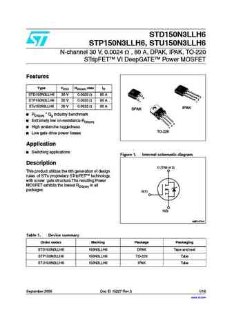
STD150N3LLH6 STP150N3LLH6, STU150N3LLH6 N-channel 30 V, 0.0024 , 80 A, DPAK, IPAK, TO-220 STripFET VI DeepGATE Power MOSFET Features Type VDSS RDS(on) max ID STD150N3LLH6 30 V 0.0028 80 A 3 3 2 STP150N3LLH6 30 V 0.0033 80 A 1 1 STu150N3LLH6 30 V 0.0033 80 A IPAK DPAK RDS(on) * Qg industry benchmark Extremely low on-resistance RDS(on) 3 2 Hi
std150nh02l-1 std150nh02lt4.pdf
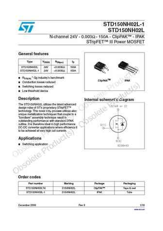
STD150NH02L-1 STD150NH02L N-channel 24V - 0.003 - 150A - ClipPAK - IPAK STripFET IlI Power MOSFET General features VDSSS RDS(on) ID Type STD150NH02L 24V
std150nh02l.pdf
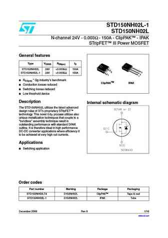
STD150NH02L-1 STD150NH02L N-channel 24V - 0.003 - 150A - ClipPAK - IPAK STripFET IlI Power MOSFET General features VDSSS RDS(on) ID Type STD150NH02L 24V
ttd1509b.pdf
TTD1509B NPN ( ) TTD1509B TTD1509B TTD1509B TTD1509B 1. 1. 1. 1. 2. 2. 2. 2. (1)
rsd150n06.pdf

Data Sheet 4V Drive Nch MOSFET RSD150N06 Structure Dimensions (Unit mm) Silicon N-channel MOSFET CPT3 (SC-63) Features 1) Low on-resistance. 2) Fast switching speed. 3) Drive circuits can be simple. 9 4) Parallel use is easy. Applications Switching Packaging specifications Inner ci
rsd150n06fra.pdf
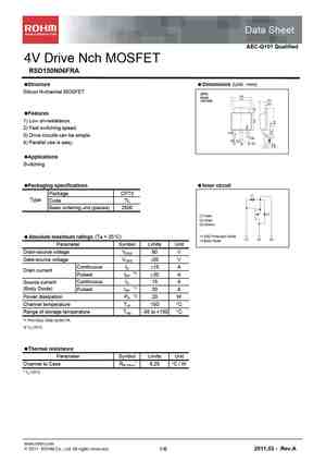
Data Sheet AEC-Q101 Qualified 4V Drive Nch MOSFET RSD150N06FRA Structure Dimensions (Unit mm) Silicon N-channel MOSFET CPT3 (SC-63) Features 1) Low on-resistance. 2) Fast switching speed. 3) Drive circuits can be simple. 9 4) Parallel use is easy. Applications Switching Packaging spec
fd150r12rt4.pdf
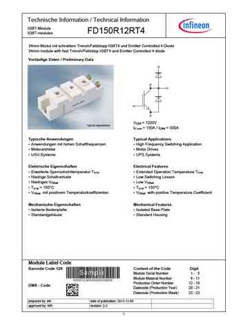
Technische Information / Technical Information IGBT-Module FD150R12RT4 IGBT-modules 34mm Modul mit schnellem Trench/Feldstopp IGBT4 und Emitter Controlled 4 Diode 34mm module with fast Trench/Fieldstop IGBT4 and Emitter Controlled 4 diode Vorl ufige Daten / Preliminary Data V = 1200V CES I = 150A / I = 300A C nom CRM Typische Anwendungen Typical Applications Anwendungen mit hoh
mid150-12a4.pdf
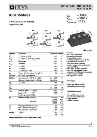
MII 150-12 A4 MID 150-12 A4 MDI 150-12 A4 IC25 = 180 A IGBT Modules VCES = 1200 V VCE(sat) typ. = 2.2 V Short Circuit SOA Capability Square RBSOA 3 MII MID MDI 2 11 3 3 3 1 10 9 8 8 8 1 1 1 9 9 11 11 2 2 2 10 10 E 72873 Features Symbol Conditions Maximum Ratings NPT IGBT technology low saturation voltage VCES TJ = 25 C to 150 C 1200 V low switching losses VCGR T
lnd150.pdf
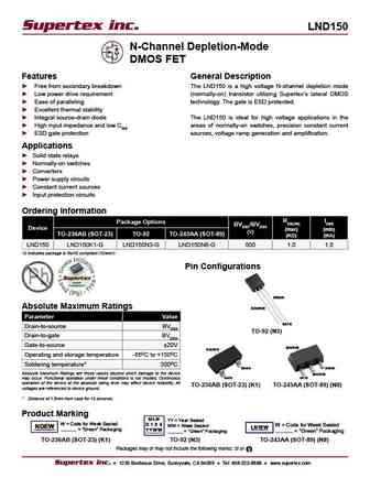
LND150 N-Channel Depletion-Mode DMOS FET Features General Description Free from secondary breakdown The LND150 is a high voltage N-channel depletion mode Low power drive requirement (normally-on) transistor utilizing Supertex s lateral DMOS Ease of paralleling technology. The gate is ESD protected. Excellent thermal stability Integral source-drain diode The LND1
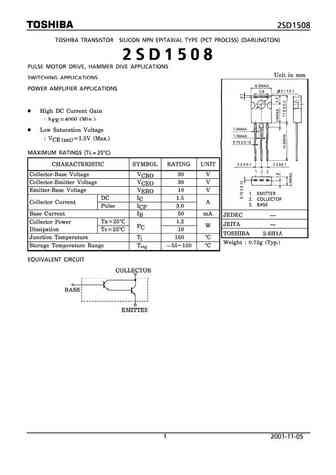
2sd1504.pdf
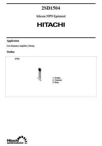
2SD1504 Silicon NPN Epitaxial Application Low frequency amplifier, Muting Outline SPAK 1. Emitter 1 2 2. Collector 3 3. Base 2SD1504 Absolute Maximum Ratings (Ta = 25 C) Item Symbol Ratings Unit Collector to base voltage VCBO 30 V Collector to emitter voltage VCEO 15 V Emitter to base voltage VEBO 5V Collector current IC 0.5 A Collector peak current ic (peak) 1.0 A Collect
csd1506.pdf
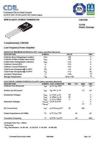
Continental Device India Limited An ISO/TS 16949, ISO 9001 and ISO 14001 Certified Company NPN PLASTIC POWER TRANSISTOR CSD1506 TO126 Plastic Package E C B Complementary CSB1065 Low Frequency Power Amplifier ABSOLUTE MAXIMUM RATINGS(Ta=25 C unless specified otherwise) DESCRIPTION SYMBOL VALUE UNIT VCBO Collector Base Voltage(open emitter) >60 V Collector Emitter Voltage (open b
pd1503yvs.pdf
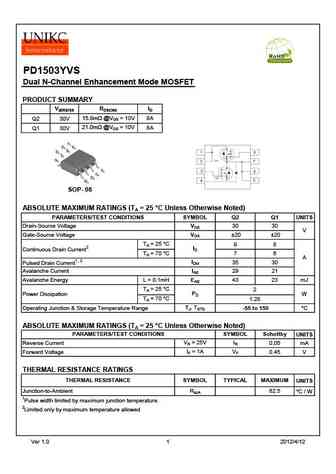
PD1503YVS Dual N-Channel Enhancement Mode MOSFET PRODUCT SUMMARY V(BR)DSS RDS(ON) ID 15.8m @VGS = 10V Q2 30V 9A 21.0m @VGS = 10V Q1 30V 8A SOP- 08 ABSOLUTE MAXIMUM RATINGS (TA = 25 C Unless Otherwise Noted) PARAMETERS/TEST CONDITIONS SYMBOL Q2 Q1 UNITS Drain-Source Voltage VDS 30 30 V Gate-Source Voltage VGS 20 20 TA = 25 C 9 8 ID Continuous Drain Current2 TA =
pd1503yvs-a.pdf
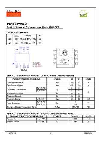
PD1503YVS-A Dual N- Channel Enhancement Mode MOSFET PRODUCT SUMMARY V(BR)DSS RDS(ON) ID 15.5m @VGS = 10V Q2 30V 9A 18m @VGS = 10V Q1 30V 8A SOP-8 ABSOLUTE MAXIMUM RATINGS (TA = 25 C Unless Otherwise Noted) PARAMETERS/TEST CONDITIONS SYMBOL Q2 Q1 UNITS VDS Drain-Source Voltage 30 30 V VGS Gate-Source Voltage 20 20 V TA = 25 C 9 8 ID Continuous Drain Current TA
pd1503bv.pdf
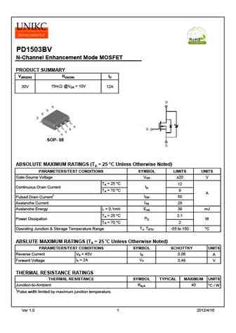
PD1503BV N-Channel Enhancement Mode MOSFET PRODUCT SUMMARY V(BR)DSS RDS(ON) ID 30V 15m @VGS = 10V 12A SOP- 08 ABSOLUTE MAXIMUM RATINGS (TA = 25 C Unless Otherwise Noted) PARAMETERS/TEST CONDITIONS SYMBOL LIMITS UNITS VGS Gate-Source Voltage 20 V TA = 25 C 12 ID Continuous Drain Current TA = 70 C 9 A IDM 50 Pulsed Drain Current1 IAS Avalanche Current 28 EAS
fhd150.pdf
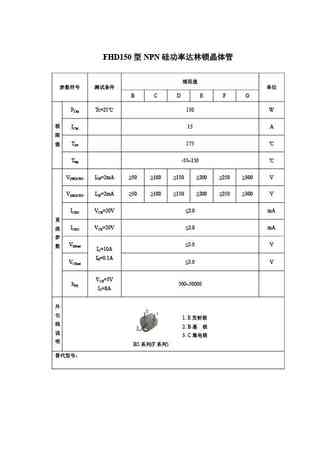
FHD150 NPN B C D E F G PCM Tc=25 150 W ICM 15 A Tjm 175 Tstg -55 150 V(BR)CBO ICB=2mA 50 100 150 200 250 300 V V(BR)CEO ICE=2mA 50 100 150 200 250 300 V ICBO VCB=20V 2.0 mA ICEO VCE=20V 2.0 mA VBEsat 3.0 V
dsd150n10l3 dsb150n10l3.pdf

DSD150N10L3&DSB150N10L3 100V/12m /60A N-MOSFET Features Key Parameters VDS Low on resistance 100V RDS(on)typ. Low reverse transfer capacitances 12m ID 100% single pulse avalanche energy test 60A Ciss@10V 100% VDS test 2320pF Pb-Free plating / Halogen-Free / RoHS compliant Qgd 7nC Applications Motor Control and Drive Charge/Discharge for Battery M
mdd1501rh.pdf

MDD1501 Single N-channel Trench MOSFET 30V, 67.4A, 5.6m General Description Features The MDD1501 uses advanced MagnaChip s MOSFET V = 30V DS Technology, which provides high performance in on-state I = 67.4A @V = 10V D GS resistance, fast switching performance and excellent R DS(ON) (MAX) quality. MDD1501 is suitable device for DC to DC
mdd1504rh.pdf
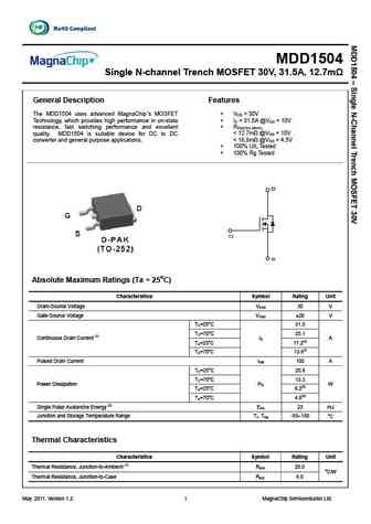
MDD1504 Single N-channel Trench MOSFET 30V, 31.5A, 12.7m Features General Description The MDD1504 uses advanced MagnaChip s MOSFET V = 30V DS Technology, which provides high performance in on-state I = 31.5A @V = 10V D GS resistance, fast switching performance and excellent R DS(ON) (MAX) quality. MDD1504 is suitable device for DC to DC
mpmd150b120rh.pdf
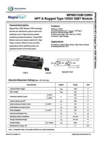
MPMD150B120RH NPT & Rugged Type 1200V IGBT Module General Description Features MagnaChip s IGBT Module 7DM-3 package BV = 1200V CES Low Conduction Loss V = 2.8V (typ.) CE(sat) devices are optimized to reduce losses and Fast & Soft Anti-Parallel FWD switching noise in high frequency power Short circuit rated Min. 10us at TC=100 Isolation Typ
mdd1502rh.pdf
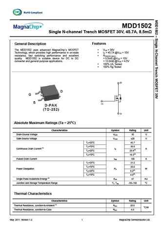
MDD1502 Single N-channel Trench MOSFET 30V, 45.7A, 8.5m General Description Features The MDD1502 uses advanced MagnaChip s MOSFET V = 30V DS Technology, which provides high performance in on-state I = 45.7A @V = 10V D GS resistance, fast switching performance and excellent R DS(ON) (MAX) quality. MDD1502 is suitable device for DC to DC
mdd1503rh.pdf
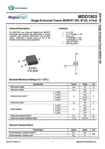
MDD1503 Single N-channel Trench MOSFET 30V, 87.5A, 4.7m Features General Description The MDD1503 uses advanced MagnaChip s MOSFET V = 30V DS Technology, which provides high performance in on-state I = 87.5A @V = 10V D GS resistance, fast switching performance and excellent R DS(ON) (MAX) quality. MDD1503 is suitable device for DC to DC
fhd150n03b.pdf
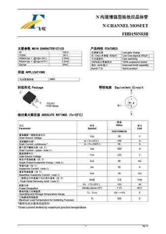
N N-CHANNEL MOSFET FHD150N03B MAIN CHARACTERISTICS FEATURES ID 150 A Low gate charge VDSS 30 V Crss ( 405pF) Low Crss (typical 405pF ) Rdson-typ @Vgs=10V 2.2m Fast switching Rdson-typ @Vgs=4.5V 2.8m 100% 100% avalanche tested Qg-typ
fhp150n03a fhs150n03a fhd150n03a.pdf
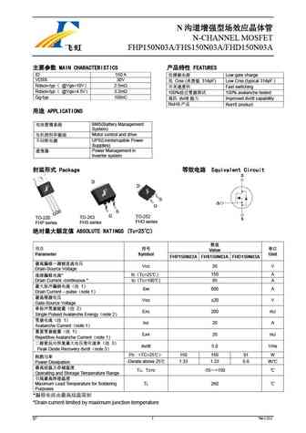
N N-CHANNEL MOSFET FHP150N03A/FHS150N03A/FHD150N03A MAIN CHARACTERISTICS FEATURES ID 150 A Low gate charge VDSS 30V Crss ( 314pF) Low Crss (typical 314pF ) Rdson-typ @Vgs=10V 2.5m Fast switching Rdson-typ @Vgs=4.5V 3.2m 100% 100% avalanc
hrld150n10k hrlu150n10k.pdf
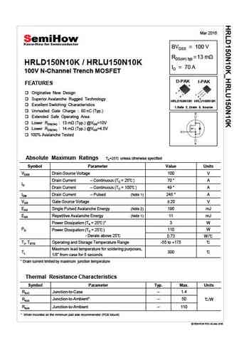
Mar 2016 BVDSS = 100 V RDS(on) typ =13 HRLD150N10K / HRLU150N10K ID = 70 A 100V N-Channel Trench MOSFET D-PAK I-PAK FEATURES 2 1 Originative New Design 1 3 2 3 Superior Avalanche Rugged Technology HRLD150N10K HRLU150N10K Excellent Switching Characteristics 1.Gate 2. Drain 3. Source Unrivalled Gate Charge 80 nC (Typ.) Extended Safe Operating Area Lower RDS(O
3cd150.pdf
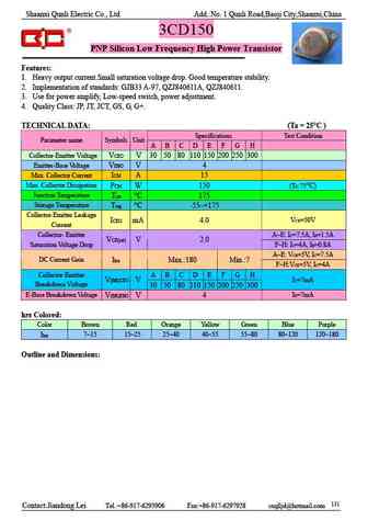
Shaanxi Qunli Electric Co., Ltd Add. No. 1 Qunli Road,Baoji City,Shaanxi,China 3CD150 PNP Silicon Low Frequency High Power Transistor Features 1. Heavy output current.Small saturation voltage drop. Good temperature stability. 2. Implementation of standards GJB33 A-97, QZJ840611A, QZJ840611. 3. Use for power amplify, Low-speed switch, power adjustment. 4. Quality Class JP, JT, JC
htd150p06.pdf
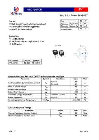
HTD150P06 P-1 60V P-Ch Power MOSFET -60 V VDS Feature 12 RDS(on),typ VGS=-10V m High Speed Power Switching, Logic Level 15 RDS(on),typ VGS=-4.5V m Enhanced Avalanche Ruggedness -40 A ID (Sillicon Limited) Lead Free, Halogen Free Application Load Switches Hard Switching and High Speed Circuit BLDC Motor TO-252 Drain 2 Gate 3 1 Part Number Pac
2sd1503.pdf
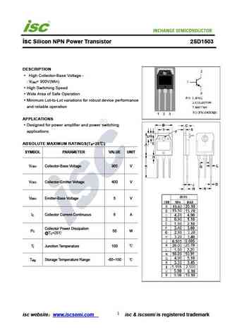
isc Product Specification isc Silicon NPN Power Transistor 2SD1503 DESCRIPTION High Collector-Base Voltage - V = 900V(Min) CBO High Switching Speed Wide Area of Safe Operation Minimum Lot-to-Lot variations for robust device performance and reliable operation APPLICATIONS Designed for power amplifier and power switching applications ABSOLUTE MAXIMUM RATINGS(T =25 ) a
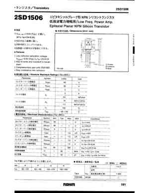
2sd1506.pdf
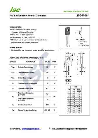
isc Silicon NPN Power Transistor 2SD1506 DESCRIPTION Low Collector Saturation Voltage V = 1.0V(Max)@I = 2A CE(sat) C Wide Area of Safe Operation Complement to Type 2SB1065 Minimum Lot-to-Lot variations for robust device performance and reliable operation APPLICATIONS Designed for low frequency power amplifier applications. ABSOLUTE MAXIMUM RATINGS(T =25 ) a SYMBOL PAR
2sd1500.pdf
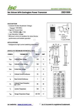
isc Silicon NPN Darlington Power Transistor 2SD1500 DESCRIPTION Collector-Emitter Breakdown Voltage- V = 100V(Min) (BR)CEO High DC Current Gain h = 1000(Min) @I = 10A FE C Low Saturation Voltage Minimum Lot-to-Lot variations for robust device performance and reliable operation APPLICATIONS Designed for high current switching applications. ABSOLUTE MAXIMUM RATINGS(T =2
2sd1505.pdf
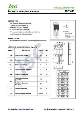
isc Silicon NPN Power Transistor 2SD1505 DESCRIPTION Low Collector Saturation Voltage V = 1.0V(Max)@I = 2A CE(sat) C Wide Area of Safe Operation Complement to Type 2SB1064 Minimum Lot-to-Lot variations for robust device performance and reliable operation APPLICATIONS Designed for low frequency power amplifier applications. ABSOLUTE MAXIMUM RATINGS(T =25 ) a SYMBOL PAR
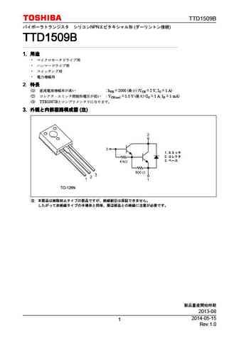
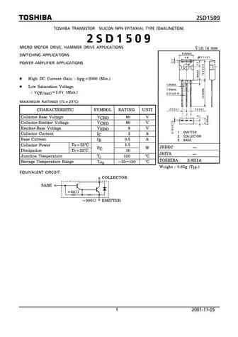
2sd1509.pdf
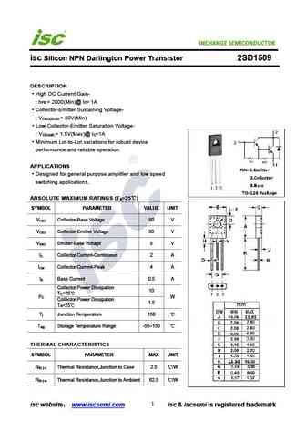
isc Silicon NPN Darlington Power Transistor 2SD1509 DESCRIPTION High DC Current Gain- h = 2000(Min)@ I = 1A FE C Collector-Emitter Sustaining Voltage- V = 80V(Min) CEO(SUS) Low Collector-Emitter Saturation Voltage- V = 1.5V(Max)@ I =1A CE(sat) C Minimum Lot-to-Lot variations for robust device performance and reliable operation APPLICATIONS Designed for general purp
Otros transistores... D11E405, D11E406, D11E407, D12E026, D12E109, D12E126, D12X043, D12X047, 2SC4793, D1666, D16E7, D16E9, D16G6, D16K1, D16K2, D16K3, D16K4
🌐 : EN ES РУ

Liste
Recientemente añadidas las descripciónes de los transistores:
BJT: GA1A4M | SBT42 | 2SA200-Y | 2SA200-O | 2SD882-Q | 2SD882-P | 2SD882-E | 2SC945-L | 2SC945-H | 2SC4226-R23 | 2SC3357-F | 2SC3357-E | 2SC3356-R26 | 2SC3356-R24 | 2SC3356-R23 | 2SB772-Q | 2SB772-P | 2SB772-E | 2SA1015-L | 2SA1015-H | HSS8550
Popular searches
tl431 datasheet | 2sd526 | 2n4403 transistor equivalent | 2sc1318 | 2n3055 transistor equivalent | 2sc1740 | c3229 | c2078 transistor