D150 Datasheet. Specs and Replacement
Type Designator: D150 📄📄
Material of Transistor: Si
Polarity: NPN
Absolute Maximum Ratings
Maximum Collector Power Dissipation (Pc): 0.5 W
Maximum Collector-Base Voltage |Vcb|: 35 V
Maximum Collector-Emitter Voltage |Vce|: 30 V
Maximum Emitter-Base Voltage |Veb|: 1 V
Maximum Collector Current |Ic max|: 1 A
Max. Operating Junction Temperature (Tj): 175 °C
Electrical Characteristics
Transition Frequency (ft): 80 MHz
Forward Current Transfer Ratio (hFE), MIN: 50
Package: TO106
D150 Substitution
- BJT ⓘ Cross-Reference Search
D150 datasheet
std150n3llh6 stp150n3llh6 stu150n3llh6.pdf ![]()
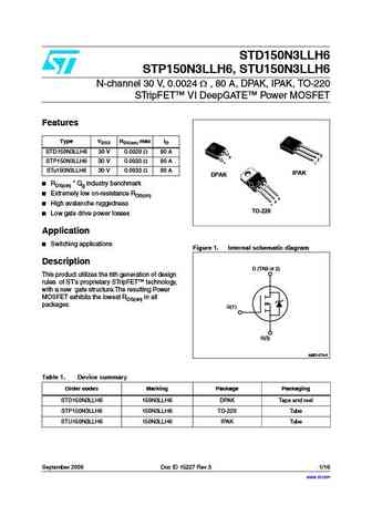
STD150N3LLH6 STP150N3LLH6, STU150N3LLH6 N-channel 30 V, 0.0024 , 80 A, DPAK, IPAK, TO-220 STripFET VI DeepGATE Power MOSFET Features Type VDSS RDS(on) max ID STD150N3LLH6 30 V 0.0028 80 A 3 3 2 STP150N3LLH6 30 V 0.0033 80 A 1 1 STu150N3LLH6 30 V 0.0033 80 A IPAK DPAK RDS(on) * Qg industry benchmark Extremely low on-resistance RDS(on) 3 2 Hi... See More ⇒
std150nh02l-1 std150nh02lt4.pdf ![]()
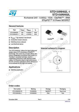
STD150NH02L-1 STD150NH02L N-channel 24V - 0.003 - 150A - ClipPAK - IPAK STripFET IlI Power MOSFET General features VDSSS RDS(on) ID Type STD150NH02L 24V ... See More ⇒
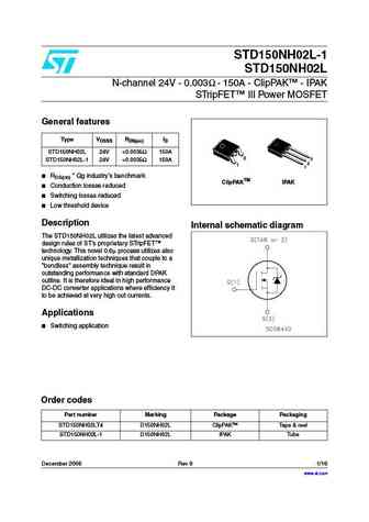
STD150NH02L-1 STD150NH02L N-channel 24V - 0.003 - 150A - ClipPAK - IPAK STripFET IlI Power MOSFET General features VDSSS RDS(on) ID Type STD150NH02L 24V ... See More ⇒
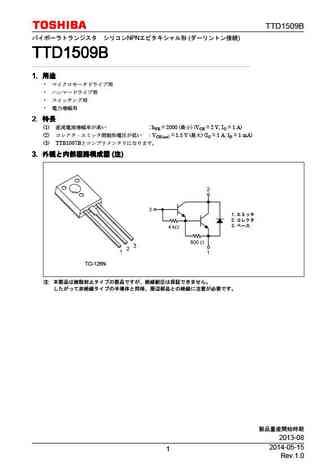
TTD1509B NPN ( ) TTD1509B TTD1509B TTD1509B TTD1509B 1. 1. 1. 1. 2. 2. 2. 2. (1) ... See More ⇒
Data Sheet 4V Drive Nch MOSFET RSD150N06 Structure Dimensions (Unit mm) Silicon N-channel MOSFET CPT3 (SC-63) Features 1) Low on-resistance. 2) Fast switching speed. 3) Drive circuits can be simple. 9 4) Parallel use is easy. Applications Switching Packaging specifications Inner ci... See More ⇒
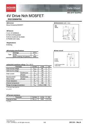
Data Sheet AEC-Q101 Qualified 4V Drive Nch MOSFET RSD150N06FRA Structure Dimensions (Unit mm) Silicon N-channel MOSFET CPT3 (SC-63) Features 1) Low on-resistance. 2) Fast switching speed. 3) Drive circuits can be simple. 9 4) Parallel use is easy. Applications Switching Packaging spec... See More ⇒
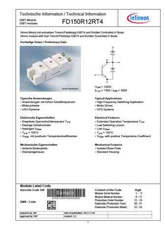
Technische Information / Technical Information IGBT-Module FD150R12RT4 IGBT-modules 34mm Modul mit schnellem Trench/Feldstopp IGBT4 und Emitter Controlled 4 Diode 34mm module with fast Trench/Fieldstop IGBT4 and Emitter Controlled 4 diode Vorl ufige Daten / Preliminary Data V = 1200V CES I = 150A / I = 300A C nom CRM Typische Anwendungen Typical Applications Anwendungen mit hoh... See More ⇒
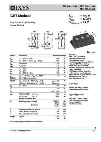
MII 150-12 A4 MID 150-12 A4 MDI 150-12 A4 IC25 = 180 A IGBT Modules VCES = 1200 V VCE(sat) typ. = 2.2 V Short Circuit SOA Capability Square RBSOA 3 MII MID MDI 2 11 3 3 3 1 10 9 8 8 8 1 1 1 9 9 11 11 2 2 2 10 10 E 72873 Features Symbol Conditions Maximum Ratings NPT IGBT technology low saturation voltage VCES TJ = 25 C to 150 C 1200 V low switching losses VCGR T... See More ⇒
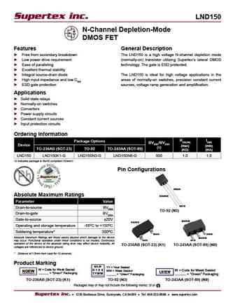
LND150 N-Channel Depletion-Mode DMOS FET Features General Description Free from secondary breakdown The LND150 is a high voltage N-channel depletion mode Low power drive requirement (normally-on) transistor utilizing Supertex s lateral DMOS Ease of paralleling technology. The gate is ESD protected. Excellent thermal stability Integral source-drain diode The LND1... See More ⇒
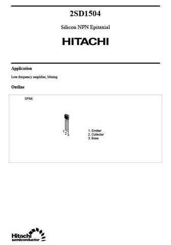
2SD1504 Silicon NPN Epitaxial Application Low frequency amplifier, Muting Outline SPAK 1. Emitter 1 2 2. Collector 3 3. Base 2SD1504 Absolute Maximum Ratings (Ta = 25 C) Item Symbol Ratings Unit Collector to base voltage VCBO 30 V Collector to emitter voltage VCEO 15 V Emitter to base voltage VEBO 5V Collector current IC 0.5 A Collector peak current ic (peak) 1.0 A Collect... See More ⇒
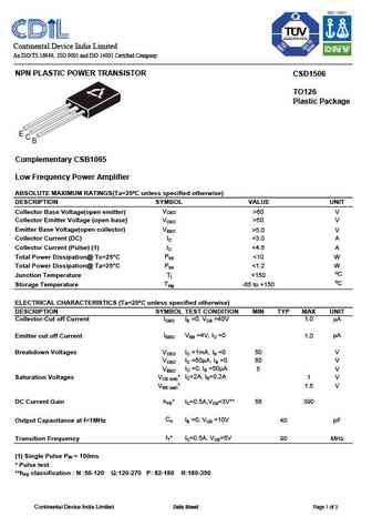
Continental Device India Limited An ISO/TS 16949, ISO 9001 and ISO 14001 Certified Company NPN PLASTIC POWER TRANSISTOR CSD1506 TO126 Plastic Package E C B Complementary CSB1065 Low Frequency Power Amplifier ABSOLUTE MAXIMUM RATINGS(Ta=25 C unless specified otherwise) DESCRIPTION SYMBOL VALUE UNIT VCBO Collector Base Voltage(open emitter) >60 V Collector Emitter Voltage (open b... See More ⇒
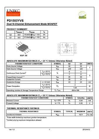
PD1503YVS Dual N-Channel Enhancement Mode MOSFET PRODUCT SUMMARY V(BR)DSS RDS(ON) ID 15.8m @VGS = 10V Q2 30V 9A 21.0m @VGS = 10V Q1 30V 8A SOP- 08 ABSOLUTE MAXIMUM RATINGS (TA = 25 C Unless Otherwise Noted) PARAMETERS/TEST CONDITIONS SYMBOL Q2 Q1 UNITS Drain-Source Voltage VDS 30 30 V Gate-Source Voltage VGS 20 20 TA = 25 C 9 8 ID Continuous Drain Current2 TA =... See More ⇒
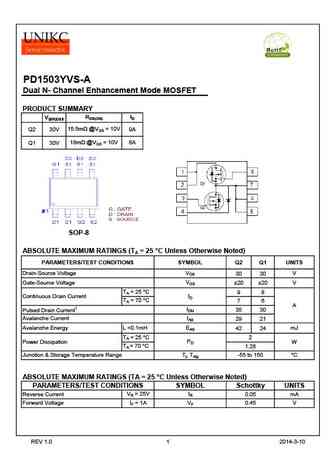
PD1503YVS-A Dual N- Channel Enhancement Mode MOSFET PRODUCT SUMMARY V(BR)DSS RDS(ON) ID 15.5m @VGS = 10V Q2 30V 9A 18m @VGS = 10V Q1 30V 8A SOP-8 ABSOLUTE MAXIMUM RATINGS (TA = 25 C Unless Otherwise Noted) PARAMETERS/TEST CONDITIONS SYMBOL Q2 Q1 UNITS VDS Drain-Source Voltage 30 30 V VGS Gate-Source Voltage 20 20 V TA = 25 C 9 8 ID Continuous Drain Current TA ... See More ⇒
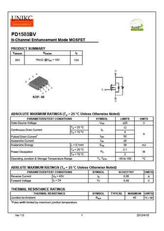
PD1503BV N-Channel Enhancement Mode MOSFET PRODUCT SUMMARY V(BR)DSS RDS(ON) ID 30V 15m @VGS = 10V 12A SOP- 08 ABSOLUTE MAXIMUM RATINGS (TA = 25 C Unless Otherwise Noted) PARAMETERS/TEST CONDITIONS SYMBOL LIMITS UNITS VGS Gate-Source Voltage 20 V TA = 25 C 12 ID Continuous Drain Current TA = 70 C 9 A IDM 50 Pulsed Drain Current1 IAS Avalanche Current 28 EAS ... See More ⇒
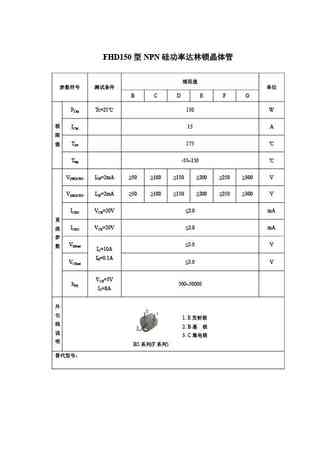
FHD150 NPN B C D E F G PCM Tc=25 150 W ICM 15 A Tjm 175 Tstg -55 150 V(BR)CBO ICB=2mA 50 100 150 200 250 300 V V(BR)CEO ICE=2mA 50 100 150 200 250 300 V ICBO VCB=20V 2.0 mA ICEO VCE=20V 2.0 mA VBEsat 3.0 V ... See More ⇒
DSD150N10L3&DSB150N10L3 100V/12m /60A N-MOSFET Features Key Parameters VDS Low on resistance 100V RDS(on)typ. Low reverse transfer capacitances 12m ID 100% single pulse avalanche energy test 60A Ciss@10V 100% VDS test 2320pF Pb-Free plating / Halogen-Free / RoHS compliant Qgd 7nC Applications Motor Control and Drive Charge/Discharge for Battery M... See More ⇒
MDD1501 Single N-channel Trench MOSFET 30V, 67.4A, 5.6m General Description Features The MDD1501 uses advanced MagnaChip s MOSFET V = 30V DS Technology, which provides high performance in on-state I = 67.4A @V = 10V D GS resistance, fast switching performance and excellent R DS(ON) (MAX) quality. MDD1501 is suitable device for DC to DC ... See More ⇒
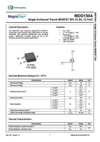
MDD1504 Single N-channel Trench MOSFET 30V, 31.5A, 12.7m Features General Description The MDD1504 uses advanced MagnaChip s MOSFET V = 30V DS Technology, which provides high performance in on-state I = 31.5A @V = 10V D GS resistance, fast switching performance and excellent R DS(ON) (MAX) quality. MDD1504 is suitable device for DC to DC ... See More ⇒
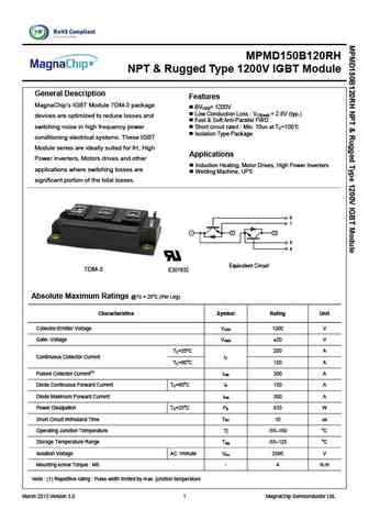
MPMD150B120RH NPT & Rugged Type 1200V IGBT Module General Description Features MagnaChip s IGBT Module 7DM-3 package BV = 1200V CES Low Conduction Loss V = 2.8V (typ.) CE(sat) devices are optimized to reduce losses and Fast & Soft Anti-Parallel FWD switching noise in high frequency power Short circuit rated Min. 10us at TC=100 Isolation Typ... See More ⇒
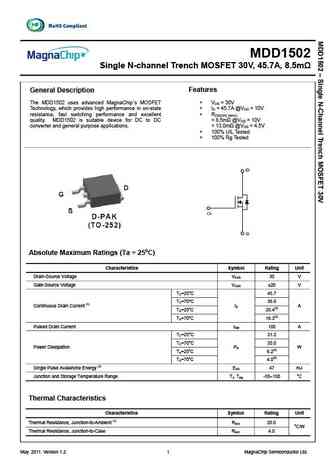
MDD1502 Single N-channel Trench MOSFET 30V, 45.7A, 8.5m General Description Features The MDD1502 uses advanced MagnaChip s MOSFET V = 30V DS Technology, which provides high performance in on-state I = 45.7A @V = 10V D GS resistance, fast switching performance and excellent R DS(ON) (MAX) quality. MDD1502 is suitable device for DC to DC ... See More ⇒
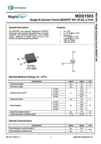
MDD1503 Single N-channel Trench MOSFET 30V, 87.5A, 4.7m Features General Description The MDD1503 uses advanced MagnaChip s MOSFET V = 30V DS Technology, which provides high performance in on-state I = 87.5A @V = 10V D GS resistance, fast switching performance and excellent R DS(ON) (MAX) quality. MDD1503 is suitable device for DC to DC ... See More ⇒
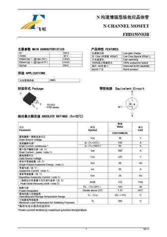
N N-CHANNEL MOSFET FHD150N03B MAIN CHARACTERISTICS FEATURES ID 150 A Low gate charge VDSS 30 V Crss ( 405pF) Low Crss (typical 405pF ) Rdson-typ @Vgs=10V 2.2m Fast switching Rdson-typ @Vgs=4.5V 2.8m 100% 100% avalanche tested Qg-typ ... See More ⇒
fhp150n03a fhs150n03a fhd150n03a.pdf ![]()
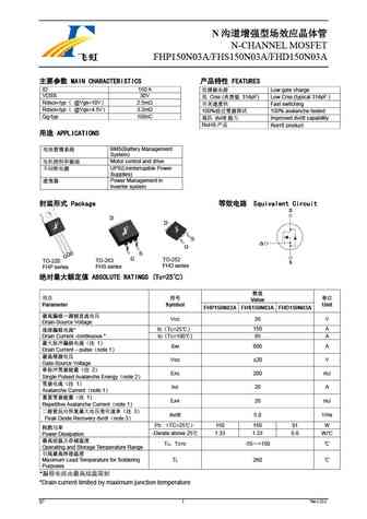
N N-CHANNEL MOSFET FHP150N03A/FHS150N03A/FHD150N03A MAIN CHARACTERISTICS FEATURES ID 150 A Low gate charge VDSS 30V Crss ( 314pF) Low Crss (typical 314pF ) Rdson-typ @Vgs=10V 2.5m Fast switching Rdson-typ @Vgs=4.5V 3.2m 100% 100% avalanc... See More ⇒
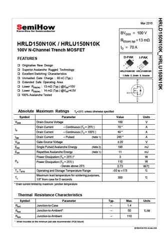
Mar 2016 BVDSS = 100 V RDS(on) typ =13 HRLD150N10K / HRLU150N10K ID = 70 A 100V N-Channel Trench MOSFET D-PAK I-PAK FEATURES 2 1 Originative New Design 1 3 2 3 Superior Avalanche Rugged Technology HRLD150N10K HRLU150N10K Excellent Switching Characteristics 1.Gate 2. Drain 3. Source Unrivalled Gate Charge 80 nC (Typ.) Extended Safe Operating Area Lower RDS(O... See More ⇒
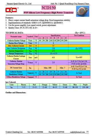
Shaanxi Qunli Electric Co., Ltd Add. No. 1 Qunli Road,Baoji City,Shaanxi,China 3CD150 PNP Silicon Low Frequency High Power Transistor Features 1. Heavy output current.Small saturation voltage drop. Good temperature stability. 2. Implementation of standards GJB33 A-97, QZJ840611A, QZJ840611. 3. Use for power amplify, Low-speed switch, power adjustment. 4. Quality Class JP, JT, JC... See More ⇒
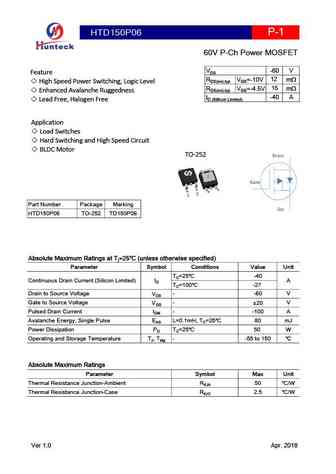
HTD150P06 P-1 60V P-Ch Power MOSFET -60 V VDS Feature 12 RDS(on),typ VGS=-10V m High Speed Power Switching, Logic Level 15 RDS(on),typ VGS=-4.5V m Enhanced Avalanche Ruggedness -40 A ID (Sillicon Limited) Lead Free, Halogen Free Application Load Switches Hard Switching and High Speed Circuit BLDC Motor TO-252 Drain 2 Gate 3 1 Part Number Pac... See More ⇒
isc Product Specification isc Silicon NPN Power Transistor 2SD1503 DESCRIPTION High Collector-Base Voltage - V = 900V(Min) CBO High Switching Speed Wide Area of Safe Operation Minimum Lot-to-Lot variations for robust device performance and reliable operation APPLICATIONS Designed for power amplifier and power switching applications ABSOLUTE MAXIMUM RATINGS(T =25 ) a... See More ⇒
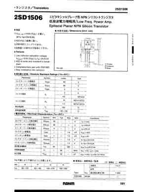
isc Silicon NPN Power Transistor 2SD1506 DESCRIPTION Low Collector Saturation Voltage V = 1.0V(Max)@I = 2A CE(sat) C Wide Area of Safe Operation Complement to Type 2SB1065 Minimum Lot-to-Lot variations for robust device performance and reliable operation APPLICATIONS Designed for low frequency power amplifier applications. ABSOLUTE MAXIMUM RATINGS(T =25 ) a SYMBOL PAR... See More ⇒
isc Silicon NPN Darlington Power Transistor 2SD1500 DESCRIPTION Collector-Emitter Breakdown Voltage- V = 100V(Min) (BR)CEO High DC Current Gain h = 1000(Min) @I = 10A FE C Low Saturation Voltage Minimum Lot-to-Lot variations for robust device performance and reliable operation APPLICATIONS Designed for high current switching applications. ABSOLUTE MAXIMUM RATINGS(T =2... See More ⇒
isc Silicon NPN Power Transistor 2SD1505 DESCRIPTION Low Collector Saturation Voltage V = 1.0V(Max)@I = 2A CE(sat) C Wide Area of Safe Operation Complement to Type 2SB1064 Minimum Lot-to-Lot variations for robust device performance and reliable operation APPLICATIONS Designed for low frequency power amplifier applications. ABSOLUTE MAXIMUM RATINGS(T =25 ) a SYMBOL PAR... See More ⇒
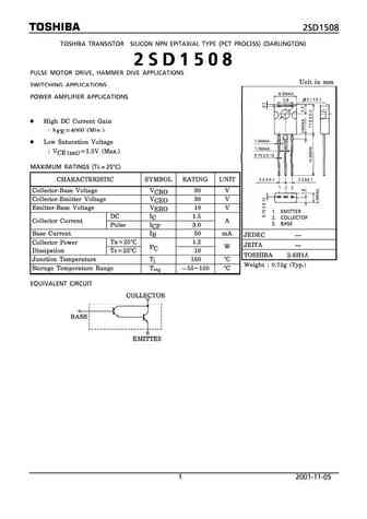
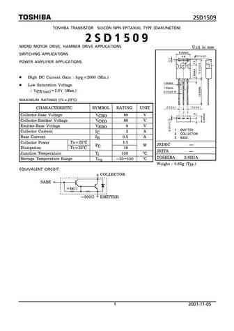
isc Silicon NPN Darlington Power Transistor 2SD1509 DESCRIPTION High DC Current Gain- h = 2000(Min)@ I = 1A FE C Collector-Emitter Sustaining Voltage- V = 80V(Min) CEO(SUS) Low Collector-Emitter Saturation Voltage- V = 1.5V(Max)@ I =1A CE(sat) C Minimum Lot-to-Lot variations for robust device performance and reliable operation APPLICATIONS Designed for general purp... See More ⇒
Detailed specifications: D11E405, D11E406, D11E407, D12E026, D12E109, D12E126, D12X043, D12X047, 2SC4793, D1666, D16E7, D16E9, D16G6, D16K1, D16K2, D16K3, D16K4
Keywords - D150 pdf specs
D150 cross reference
D150 equivalent finder
D150 pdf lookup
D150 substitution
D150 replacement
History: D16E9 | D16K1
🌐 : EN ES РУ
LIST
Last Update
BJT: GA1A4M | SBT42 | 2SA200-Y | 2SA200-O | 2SD882-Q | 2SD882-P
Popular searches
tl431 datasheet | 2sd526 | 2n4403 transistor equivalent | 2sc1318 | 2n3055 transistor equivalent | 2sc1740 | c3229 | c2078 transistor
