W21 Datasheet. Equivalente. Reemplazo. Hoja de especificaciones. Principales características
Número de Parte: W21 📄📄
Material: Si
Polaridad de transistor: PNP
ESPECIFICACIONES MÁXIMAS
Disipación total del dispositivo (Pc): 0.36 W
Tensión colector-base (Vcb): 40 V
Tensión colector-emisor (Vce): 40 V
Tensión emisor-base (Veb): 5 V
Corriente del colector DC máxima (Ic): 0.2 A
Temperatura operativa máxima (Tj): 150 °C
CARACTERÍSTICAS ELÉCTRICAS
Transición de frecuencia (fT): 200 MHz
Capacitancia de salida (Cc): 4.5 pF
Ganancia de corriente contínua (hFE): 50
📄📄 Copiar
Búsqueda de reemplazo de W21
- Selecciónⓘ de transistores por parámetros
W21 datasheet
0.1. Size:150K motorola
mjw21192 mjw21191.pdf 
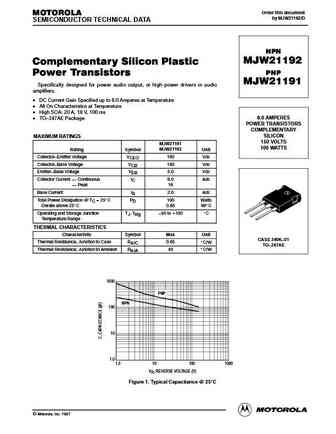
Order this document MOTOROLA by MJW21192/D SEMICONDUCTOR TECHNICAL DATA NPN MJW21192 Complementary Silicon Plastic PNP Power Transistors MJW21191 Specifically designed for power audio output, or high power drivers in audio amplifiers. DC Current Gain Specified up to 8.0 Amperes at Temperature All On Characteristics at Temperature High SOA 20 A, 18 V, 100 ms 8.0 AMPER
0.2. Size:152K motorola
mgw21n60edrev0.pdf

MOTOROLA Order this document SEMICONDUCTOR TECHNICAL DATA by MGW21N60ED/D Preliminary Data Sheet MGW21N60ED Insulated Gate Bipolar Transistor N Channel Enhancement Mode Silicon Gate This Insulated Gate Bipolar Transistor (IGBT) is co packaged IGBT IN TO 247 with a soft recovery ultra fast rectifier and uses an advanced 21 A @ 90 C termination scheme to provide an enhanced
0.3. Size:157K motorola
mgw21n60ed.pdf

MOTOROLA Order this document SEMICONDUCTOR TECHNICAL DATA by MGW21N60ED/D Designer's Data Sheet MGW21N60ED Insulated Gate Bipolar Transistor N Channel Enhancement Mode Silicon Gate This Insulated Gate Bipolar Transistor (IGBT) is co packaged IGBT IN TO 247 with a soft recovery ultra fast rectifier and uses an advanced 21 A @ 90 C termination scheme to provide an enhanc
0.4. Size:463K st
stw21nm50n.pdf

STP/F21NM50N - STW21NM50N STB21NM50N - STB21NM50N-1 N-channel 500V - 0.15 - 18A TO-220/FP/D2/I2PAK/TO-247 Second generation MDmesh Power MOSFET General features VDSS Type RDS(on) ID 3 (@Tjmax) 3 1 3 2 2 1 1 STB21NM50N 550V
0.5. Size:561K st
stp21nm60n stf21nm60n stb21nm60n stb21nm60n-1 stw21nm60n.pdf

STP21NM60N-F21NM60N-STW21NM60N STB21NM60N-STB21NM60N-1 N-channel 600 V - 0.17 - 17 A TO-220 - TO-220FP - D2PAK - I2PAK - TO-247 second generation MDmesh Power MOSFET Features VDSS RDS(on) Type ID (@Tjmax) max 3 3 3 2 1 2 1 STB21NM60N 650 V
0.6. Size:564K st
stb21nm60n-1 stb21nm60n stf21nm60n stp21nm60n stw21nm60n.pdf

STP21NM60N-F21NM60N-STW21NM60N STB21NM60N-STB21NM60N-1 N-channel 600 V - 0.17 - 17 A TO-220 - TO-220FP - D2PAK - I2PAK - TO-247 second generation MDmesh Power MOSFET Features VDSS RDS(on) Type ID (@Tjmax) max 3 3 3 2 1 2 1 STB21NM60N 650 V
0.8. Size:461K st
stp21nm50n stf21nm50n stb21nm50n stb21nm50n-1 stw21nm50n.pdf

STP/F21NM50N - STW21NM50N STB21NM50N - STB21NM50N-1 N-channel 500V - 0.15 - 18A TO-220/FP/D2/I2PAK/TO-247 Second generation MDmesh Power MOSFET General features VDSS Type RDS(on) ID 3 (@Tjmax) 3 1 3 2 2 1 1 STB21NM50N 550V
0.9. Size:1389K st
stb21nm60nd stf21nm60nd stp21nm60nd stw21nm60nd.pdf
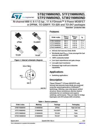
STB21NM60ND, STF21NM60ND, STP21NM60ND, STW21NM60ND N-channel 600 V, 0.17 typ., 17 A FDmesh II Power MOSFET in D PAK, TO-220FP, TO-220 and TO-247 packages Datasheet - production data Features TAB VDSS @ RDS(on) Order codes ID TJmax max 3 3 1 2 1 STB21NM60ND 650 V 0.22 17 A D2PAK TO-220FP STF21NM60ND 650 V 0.22 17 A STP21NM60ND 650 V 0.22 17 A TAB STW21NM60N
0.10. Size:1270K st
stb21n65m5 stf21n65m5 sti21n65m5 stp21n65m5 stw21n65m5.pdf

STB21N65M5, STF21N65M5 STI21N65M5, STP21N65M5, STW21N65M5 N-channel 650 V, 0.175 , 17 A MDmesh V Power MOSFET D2PAK, TO-220FP, TO-220, I2PAK, TO-247 Features VDSS @ RDS(on) Type ID PW TJmax max 3 2 3 1 STB21N65M5 17 A 125 W 2 1 TO-220 STF21N65M5 17 A(1) 30 W I PAK STI21N65M5 710 V
0.11. Size:507K st
stb21n90k5 stf21n90k5 stp21n90k5 stw21n90k5.pdf

STB21N90K5, STF21N90K5, STP21N90K5, STW21N90K5 N-channel 900 V, 0.25 typ., 18.5 A Zener-protected SuperMESH 5 Power MOSFET in a D2PAK, TO-220FP, TO-220 and TO-247 packages Datasheet production data Features TAB Order codes VDSS RDS(on)max ID PW 3 3 1 STB21N90K5 250 W 2 1 D2PAK TO-220FP STF21N90K5 40 W 900 V
0.12. Size:45K sanyo
fw213.pdf

Ordering number EN5908 P-Channel Silicon MOSFET FW213 DC-DC Converter Applications Features Package Dimensions Low ON resistance. unit mm 4V drive. 2129 [FW213] 8 5 1 Source1 2 Gate1 14 3 Source2 0.2 5.0 4 Gate2 5 Drain2 6 Drain2 7 Drain1 8 Drain1 0.595 1.27 Specifications 0.43 SANYO SOP8 Absolute Maximum Ratings at Ta = 25 C Parameter Symbol Conditions Ratings
0.13. Size:45K sanyo
fw214.pdf

Ordering number EN5850 N-Channel Silicon MOS FET FW214 Ultrahigh-Speed Switching Applications Features Package Dimensions Low ON resistance. unit mm 2.5V drive. 2129 [FW214] 8 5 1 Source1 2 Gate1 3 Source2 4 Gate2 14 0.2 5 Drain2 5.0 6 Drain2 7 Drain1 8 Drain1 0.595 1.27 0.43 SANYO SOP8 Specifications Absolute Maximum Ratings at Ta = 25 C Parameter Symbol Co
0.14. Size:44K sanyo
fw211.pdf
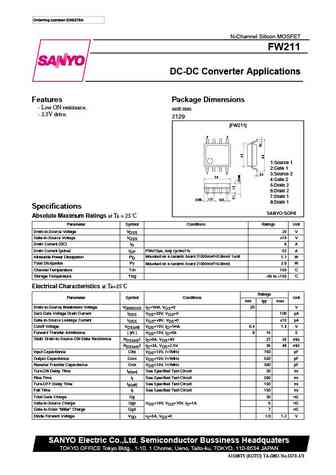
Ordering number EN5579A N-Channel Silicon MOSFET FW211 DC-DC Converter Applications Features Package Dimensions Low ON resistance. unit mm 2.5V drive. 2129 [FW211] 8 5 1 Source 1 2 Gate 1 1 4 3 Source 2 0.2 5.0 4 Gate 2 5 Drain 2 6 Drain 2 7 Drain 1 1.27 0.595 0.43 8 Drain 1 Specifications SANYO SOP8 Absolute Maximum Ratings at Ta = 25 C Parameter Symbol Cond
0.15. Size:42K sanyo
fw215.pdf

Ordering number EN5481 N-Channel Silicon MOSFET FW215 DC-DC Converter Applications Features Package Dimensions Low ON resistance. unit mm 4V drive. 2129 [FW215] 8 5 1 Source 1 2 Gate 1 3 Source 2 14 0.2 5.0 4 Gate 2 5 Drain 2 6 Drain 2 7 Drain 1 8 Drain 1 Specifications 0.595 1.27 0.43 SANYO SOP8 Absolute Maximum Ratings at Ta = 25 C Parameter Symbol Condition
0.17. Size:157K onsemi
mjw21195 mjw21196.pdf
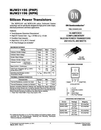
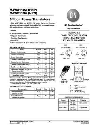
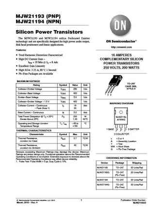
MJW21195 (PNP) MJW21196 (NPN) Silicon Power Transistors The MJW21195 and MJW21196 utilize Perforated Emitter technology and are specifically designed for high power audio output, disk head positioners and linear applications. http //onsemi.com Features 16 AMPERES Total Harmonic Distortion Characterized High DC Current Gain - hFE = 20 Min @ IC = 8 Adc COMPLEMENTARY Excell
0.18. Size:155K onsemi
mjw21192 mjw21191.pdf
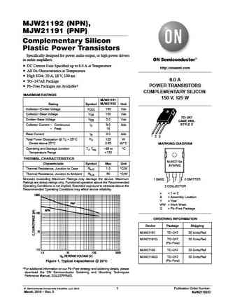
MJW21192 (NPN), MJW21191 (PNP) Complementary Silicon Plastic Power Transistors Specifically designed for power audio output, or high power drivers in audio amplifiers. DC Current Gain Specified up to 8.0 A at Temperature http //onsemi.com All On Characteristics at Temperature High SOA 20 A, 18 V, 100 ms 8.0 A TO-247AE Package POWER TRANSISTORS Pb-Free Packages
0.19. Size:90K onsemi
njw21193 njw21194.pdf
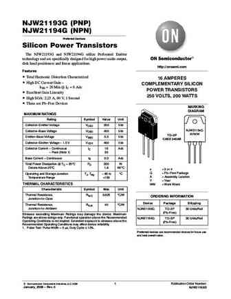
NJW21193G (PNP) NJW21194G (NPN) Preferred Devices Silicon Power Transistors The NJW21193G and NJW21194G utilize Perforated Emitter technology and are specifically designed for high power audio output, disk head positioners and linear applications. http //onsemi.com Features Total Harmonic Distortion Characterized 16 AMPERES High DC Current Gain - COMPLEMENTARY SILICON hFE
0.20. Size:153K onsemi
mjw21195g.pdf

MJW21195 (PNP) MJW21196 (NPN) Silicon Power Transistors The MJW21195 and MJW21196 utilize Perforated Emitter technology and are specifically designed for high power audio output, disk head positioners and linear applications. http //onsemi.com Features 16 AMPERES Total Harmonic Distortion Characterized High DC Current Gain - hFE = 20 Min @ IC = 8 Adc COMPLEMENTARY Excell
0.21. Size:153K onsemi
mjw21196g.pdf

MJW21195 (PNP) MJW21196 (NPN) Silicon Power Transistors The MJW21195 and MJW21196 utilize Perforated Emitter technology and are specifically designed for high power audio output, disk head positioners and linear applications. http //onsemi.com Features 16 AMPERES Total Harmonic Distortion Characterized High DC Current Gain - hFE = 20 Min @ IC = 8 Adc COMPLEMENTARY Excell
0.22. Size:117K onsemi
njw21193g njw21194g.pdf
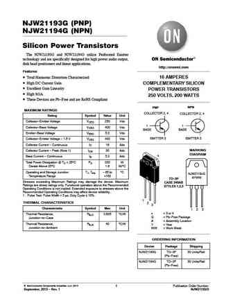
NJW21193G (PNP) NJW21194G (NPN) Silicon Power Transistors The NJW21193G and NJW21194G utilize Perforated Emitter technology and are specifically designed for high power audio output, disk head positioners and linear applications. http //onsemi.com Features Total Harmonic Distortion Characterized 16 AMPERES High DC Current Gain COMPLEMENTARY SILICON Excellent Gain Linearit
0.23. Size:268K onsemi
fw217a.pdf

Ordering number EN8994B FW217A N-Channel Power MOSFET http //onsemi.com 35V, 6A, 39m , Dual SOIC8 Features On-state resistance RDS(on)1=30m (typ.) 4.5V drive Halogen free compliance Protection Diode in Specifications Absolute Maximum Ratings at Ta=25 C Parameter Symbol Conditions Ratings Unit Drain-to-Source Voltage VDSS 35 V Gate-to-Source Voltage VGS
0.24. Size:186K onsemi
fw216a.pdf

Ordering number ENA0176C FW216A N-Channel Power MOSFET http //onsemi.com 35V, 4.5A, 64m , Dual SOIC8 Features ON-resistance Nch RDS(on)1=49m (typ.) 4.0V drive Halogen free compliance Protection diode in Specifications Absolute Maximum Ratings at Ta=25 C Parameter Symbol Conditions Ratings Unit Drain to Source Voltage VDSS 35 V Gate to Source Voltage
0.25. Size:119K onsemi
mjw21193 mjw21194.pdf
MJW21193 (PNP) MJW21194 (NPN) Silicon Power Transistors The MJW21193 and MJW21194 utilize Perforated Emitter technology and are specifically designed for high power audio output, disk head positioners and linear applications. http //onsemi.com Features 16 AMPERES Total Harmonic Distortion Characterized COMPLEMENTARY SILICON High DC Current Gain POWER TRANSISTORS Excelle
0.26. Size:121K onsemi
njw21193g-94g.pdf

NJW21193G (PNP) NJW21194G (NPN) Silicon Power Transistors The NJW21193G and NJW21194G utilize Perforated Emitter technology and are specifically designed for high power audio output, disk head positioners and linear applications. http //onsemi.com Features Total Harmonic Distortion Characterized 16 AMPERES High DC Current Gain COMPLEMENTARY SILICON Excellent Gain Linearit
0.27. Size:141K onsemi
mjw21194g.pdf

MJW21193 (PNP) MJW21194 (NPN) Silicon Power Transistors The MJW21193 and MJW21194 utilize Perforated Emitter technology and are specifically designed for high power audio output, disk head positioners and linear applications. http //onsemi.com Features Total Harmonic Distortion Characterized 16 AMPERES High DC Current Gain - COMPLEMENTARY SILICON hFE = 20 Min @ IC = 8 Adc P
0.28. Size:141K onsemi
mjw21193g.pdf
MJW21193 (PNP) MJW21194 (NPN) Silicon Power Transistors The MJW21193 and MJW21194 utilize Perforated Emitter technology and are specifically designed for high power audio output, disk head positioners and linear applications. http //onsemi.com Features Total Harmonic Distortion Characterized 16 AMPERES High DC Current Gain - COMPLEMENTARY SILICON hFE = 20 Min @ IC = 8 Adc P
0.29. Size:111K savantic
mjw21191.pdf
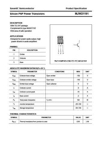
SavantIC Semiconductor Product Specification Silicon PNP Power Transistors MJW21191 DESCRIPTION With TO-247 package Complement to type MJW21192 Wild area of safe operation APPLICATIONS Designed for power audio output, high power drivers in audio amplifiers PINNING PIN DESCRIPTION 1 Emitter 2 Collector 3 Base ABSOLUTE MAXIMUM RATINGS(Tc=25 ) SYMBOL PARAMETER
0.30. Size:110K savantic
mjw21192.pdf

SavantIC Semiconductor Product Specification Silicon NPN Power Transistors MJW21192 DESCRIPTION With TO-247 package Complement to type MJW21191 Wild area of safe operation APPLICATIONS Designed for power audio output, high power drivers in audio amplifiers PINNING PIN DESCRIPTION 1 Base 2 Collector Fig.1 simplified outline (TO-247) and symbol 3 Emitter ABSOL
0.31. Size:444K cn evvo
njw21194g.pdf

NJW21194G Transistor Silicon NPN Triple Diffused Type Power Amplifier Applications Complementary to NJW21193G High collector voltage VCEO=250V (min) Recommended for 100-W high-fidelity audio frequency amplifier Output stage Note1 Using continuously under heavy loads (e.g. the application of high temperature/current/voltage and the significant change in temperature, etc.) m
0.32. Size:504K cn evvo
njw21193g.pdf

NJW21193G Transistor Silicon PNP Epitaxial Type Power Amplifier Applications Complementary to NJW21194G High collector voltage VCEO=-250V (min) Recommended for 100-W high-fidelity audio frequency amplifier Output stage Note Using continuously under heavy loads (e.g. the application of high temperature/current/voltage and the significant change in temperature, etc.) may cau
0.33. Size:217K inchange semiconductor
njw21194g.pdf
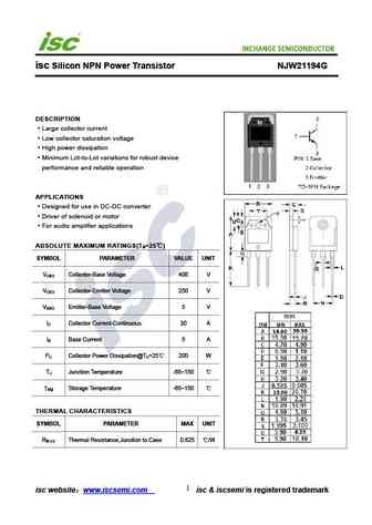
isc Silicon NPN Power Transistor NJW21194G DESCRIPTION Large collector current Low collector saturation voltage High power dissipation Minimum Lot-to-Lot variations for robust device performance and reliable operation APPLICATIONS Designed for use in DC-DC converter Driver of solenoid or motor For audio amplifier applications ABSOLUTE MAXIMUM RATINGS(T =25 ) a SYMBO
0.34. Size:222K inchange semiconductor
mjw21191.pdf
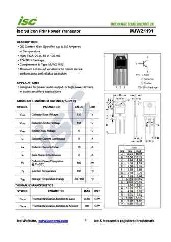
isc Silicon PNP Power Transistor MJW21191 DESCRIPTION DC Current Gain Specified up to 8.0 Amperes at Temperature High SOA 20 A, 18 V, 100 ms TO 3PN Package Complement to Type MJW21192 Minimum Lot-to-Lot variations for robust device performance and reliable operation APPLICATIONS designed for power audio output, or high power drivers in audio amplifiers applications AB
0.35. Size:203K inchange semiconductor
njw21193g.pdf
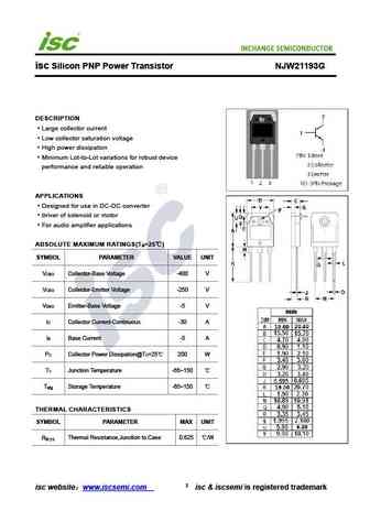
isc Silicon PNP Power Transistor NJW21193G DESCRIPTION Large collector current Low collector saturation voltage High power dissipation Minimum Lot-to-Lot variations for robust device performance and reliable operation APPLICATIONS Designed for use in DC-DC converter Driver of solenoid or motor For audio amplifier applications ABSOLUTE MAXIMUM RATINGS(T =25 ) a SYMBO
0.36. Size:178K inchange semiconductor
bdw21.pdf
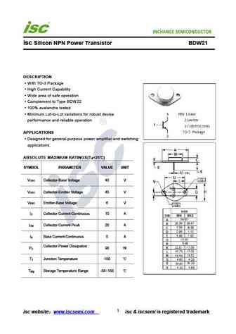
INCHANGE Semiconductor isc Silicon NPN Power Transistor BDW21 DESCRIPTION With TO-3 Package High Current Capability Wide area of safe operation Complement to Type BDW22 100% avalanche tested Minimum Lot-to-Lot variations for robust device performance and reliable operation APPLICATIONS Designed for general-purpose power amplifier and switching applications. ABSOLUTE M
0.37. Size:220K inchange semiconductor
mjw21194.pdf
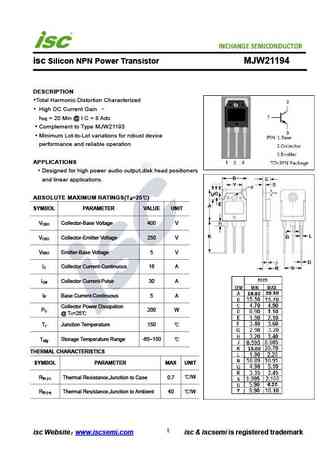
isc Silicon NPN Power Transistor MJW21194 DESCRIPTION Total Harmonic Distortion Characterized High DC Current Gain h = 20 Min @ I C = 8 Adc FE Complement to Type MJW21193 Minimum Lot-to-Lot variations for robust device performance and reliable operation APPLICATIONS Designed for high power audio output,disk head positioners and linear applications. ABSOLUTE MAXIMUM
0.38. Size:218K inchange semiconductor
mjw21193.pdf

isc Silicon PNP Power Transistor MJW21193 DESCRIPTION Total Harmonic Distortion Characterized High DC Current Gain h = 20 Min @ I C = -8 Adc FE Complement to Type MJW21194 Minimum Lot-to-Lot variations for robust device performance and reliable operation APPLICATIONS Designed for high power audio output,disk head positioners and linear applications. ABSOLUTE MAXIMUM
0.39. Size:218K inchange semiconductor
mjw21192.pdf
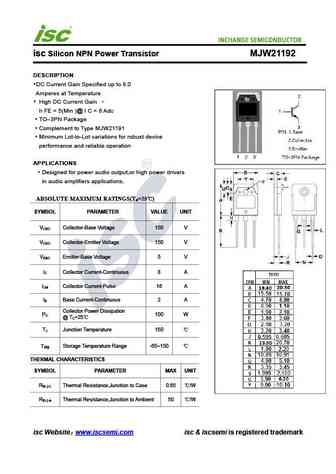
isc Silicon NPN Power Transistor MJW21192 DESCRIPTION DC Current Gain Specified up to 8.0 Amperes at Temperature High DC Current Gain h FE = 5(Min )@ I C = 8 Adc TO 3PN Package Complement to Type MJW21191 Minimum Lot-to-Lot variations for robust device performance and reliable operation APPLICATIONS Designed for power audio output,or high power drivers in audio
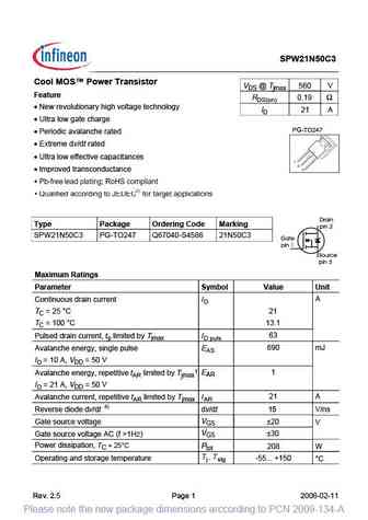
0.40. Size:244K inchange semiconductor
spw21n50c3.pdf

isc N-Channel MOSFET Transistor SPW21N50C3 ISPW21N50C3 FEATURES Static drain-source on-resistance RDS(on) 190m Enhancement mode 100% avalanche tested Minimum Lot-to-Lot variations for robust device performance and reliable operation DESCRITION Improved Transconductance ABSOLUTE MAXIMUM RATINGS(T =25 ) a SYMBOL PARAMETER VALUE UNIT V Drain-Source Voltage 50
Otros transistores... V162A, V221, V405A, V405AL, V410A, V435, V741, V765, TIP32C, WT4301-06, WT4311-16, WT4321-25, WT4331-34, WT5101-09, WT5201-15, WT5301, WT5501-05