DP100 Equivalente. Reemplazo. Hoja de especificaciones. Principales características
Número de Parte: DP100
Material: Si
Polaridad de transistor: PNP
ESPECIFICACIONES MÁXIMAS
Disipación total del dispositivo (Pc): 0.625 W
Tensión colector-base (Vcb): 15 V
Tensión colector-emisor (Vce): 12 V
Tensión emisor-base (Veb): 5 V
Corriente del colector DC máxima (Ic): 1 A
Temperatura operativa máxima (Tj): 150 °C
CARACTERÍSTICAS ELÉCTRICAS
Transición de frecuencia (fT): 330 MHz
Capacitancia de salida (Cc): 9 pF
Ganancia de corriente contínua (hFE): 200
Encapsulados: TO-92
Búsqueda de reemplazo de DP100
- Selecciónⓘ de transistores por parámetros
DP100 datasheet
dp100.pdf
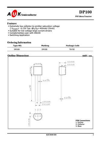
DP100 Semiconductor Semiconductor PNP Silicon Transistor Features Extremely low collector-to-emitter saturation voltage ( VCE(SAT)= -0.25V Typ. @IC/IB=-400mA/-20mA) Suitable for low voltage large current drivers Complementary pair with DN100 Switching Application Ordering Information Type NO. Marking Package Code DP100 DP100 TO-92 Outline Dimension
fdp100n10.pdf
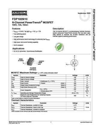
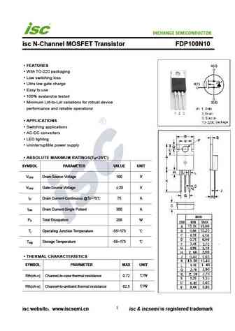
September 2009 FDP100N10 tm N-Channel PowerTrench MOSFET 100V, 75A, 10m Features Description RDS(on) = 8.2m ( Typ.)@ VGS = 10V, ID = 75A This N-Channel MOSFET is producedusing Fairchild Semicon- ductor s advanced PowerTrench process that has been espe- Fast switching speed cially tailored to minimize the on-state resistance and yet maintain superior switching perfo
dp100s.pdf
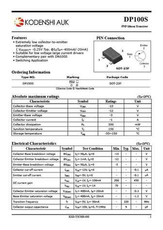
DP100S PNP Silicon Transistor Features PIN Connection Extremely low collector-to-emitter saturation voltage ( VCE(SAT)= -0.25V Typ. @IC/IB=-400mA/-20mA) 3 Suitable for low voltage large current drivers Complementary pair with DN100S 1 Switching Application 2 SOT-23F Ordering Information Type NO. Marking Package Code P03 DP100S SOT-23F
ppmdp100v10.pdf
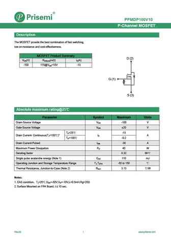
PPMDP100V10 P-Channel MOSFET Description The MOSFET provide the best combination of fast switching, low on-resistance and cost-effectiveness. MOSFET Product Summary D (2) VDS(V) RDS(on)(m ) ID(A) -100 170@VGS=10V -13 G (1) S (3) Absolute maximum rating@25 Parameter Symbol Maximum Units Drain-Source Voltage VDS -100 V Gate-Source Voltage VGS 20 V TA=25 -13

Otros transistores... DN200F, DN500, DN500F, DN500P, DP030, DP030E, DP030S, DP030U, BD139, DP100S, DP500, DP500F, DP500P, MMBT3904EF, MMBT3906EF, NT331, NT332
🌐 : EN ES РУ

Liste
Recientemente añadidas las descripciónes de los transistores:
BJT: GA1A4M | SBT42 | 2SA200-Y | 2SA200-O | 2SD882-Q | 2SD882-P | 2SD882-E | 2SC945-L | 2SC945-H | 2SC4226-R23 | 2SC3357-F | 2SC3357-E | 2SC3356-R26 | 2SC3356-R24 | 2SC3356-R23 | 2SB772-Q | 2SB772-P | 2SB772-E | 2SA1015-L | 2SA1015-H | HSS8550
Popular searches
bd139 | 2n4401 datasheet | irf640 | irf840 | irf740 | c945 transistor | irf640n | 2n3904