DMA30401 Datasheet. Equivalente. Reemplazo. Hoja de especificaciones. Principales características
Número de Parte: DMA30401 📄📄
Código: A7
Material: Si
Polaridad de transistor: PNP
ESPECIFICACIONES MÁXIMAS
Disipación total del dispositivo (Pc): 0.125 W
Tensión colector-base (Vcb): 60 V
Tensión colector-emisor (Vce): 50 V
Tensión emisor-base (Veb): 7 V
Corriente del colector DC máxima (Ic): 0.1 A
Temperatura operativa máxima (Tj): 150 °C
CARACTERÍSTICAS ELÉCTRICAS
Transición de frecuencia (fT): 150 MHz
Capacitancia de salida (Cc): 2 pF
Ganancia de corriente contínua (hFE): 210
Encapsulados: SSSMINI6-F2-B
📄📄 Copiar
Búsqueda de reemplazo de DMA30401
- Selecciónⓘ de transistores por parámetros
DMA30401 datasheet
dma30401.pdf
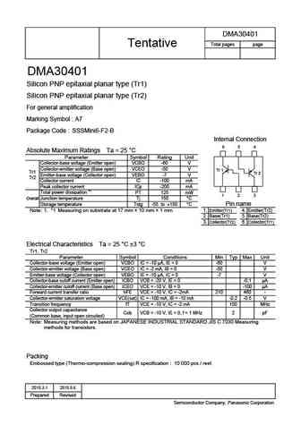
DMA30401 Total pages page Tentative DMA30401 Silicon PNP epitaxial planar type (Tr1) Silicon PNP epitaxial planar type (Tr2) For general amplification Marking Symbol A7 Package Code SSSMini6-F2-B Internal Connection 6 5 4 Absolute Maximum Ratings Ta = 25 C Parameter Symbol Rating Unit Collector-base voltage (Emitter open) VCBO -60 V Collector-emitter voltage (Base open) VC
fdma3023pz.pdf
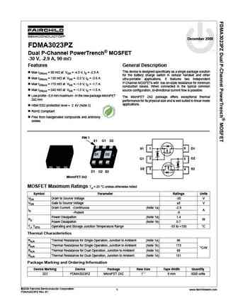
December 2008 FDMA3023PZ tm Dual P-Channel PowerTrench MOSFET -30 V, -2.9 A, 90 m Features General Description This device is designed specifically as a single package solution Max rDS(on) = 90 m at VGS = -4.5 V, ID = -2.9 A for the battery charge switch in cellular handset and other Max rDS(on) = 130 m at VGS = -2.5 V, ID = -2.6 A ultra-portable applications. It featu
fdma3027pz.pdf
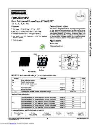
June 2012 FDMA3027PZ Dual P-Channel PowerTrench MOSFET -30 V, -3.3 A, 87 m Features General Description This device is designed specifically as a single package solution Max rDS(on) = 87 m at VGS = -10 V, ID = -3.3 A for dual switching requirements such as gate driver for larger Max rDS(on) = 152 m at VGS = -4.5 V, ID = -2.3 A Mosfets. It features two independent P-Channel
fdma3028n.pdf
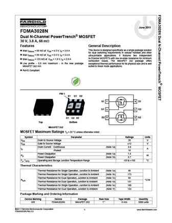
June 2011 FDMA3028N Dual N-Channel PowerTrench MOSFET 30 V, 3.8 A, 68 m Features General Description This device is designed specifically as a single package solution Max rDS(on) = 68 m at VGS = 4.5 V, ID = 3.8 A for dual switching requirements in cellular handset and other Max rDS(on) = 88 m at VGS = 2.5 V, ID = 3.4 A ultra-portable applications. It features two independe
Otros transistores... FHD491, FHD50, FHD6058, FHD651, FHD70, FHD8766, FJB5555, FJL6920, S9018, DMA90401, DMC30401, DMC90401, DMC904F0, DMC904F1, DME20101, DME20102, DME20501
Parámetros del transistor bipolar y su interrelación.
History: BD939F | DTC115EM | KRC413V | MUN5316DW1 | NB123H | KRC453 | RN1611
🌐 : EN ES РУ

Liste
Recientemente añadidas las descripciónes de los transistores:
BJT: ZDT6705 | GA1L4Z | GA1A4M | SBT42 | 2SA200-Y | 2SA200-O | 2SD882-Q | 2SD882-P | 2SD882-E | 2SC945-L | 2SC945-H | 2SC4226-R23 | 2SC3357-F | 2SC3357-E | 2SC3356-R26 | 2SC3356-R24 | 2SC3356-R23 | 2SB772-Q | 2SB772-P | 2SB772-E | 2SA1015-L
Popular searches
2sa1695 | a1175 transistor | 2sc1678 | irf4115 | 2sc828 replacement | 2sd669 datasheet | c102 transistor | bt152 datasheet