STP65NF06 Datasheet. Specs and Replacement
Type Designator: STP65NF06 📄📄
Type of Transistor: MOSFET
Type of Control Channel: N-Channel
Absolute Maximum Ratings
Pd ⓘ - Maximum Power Dissipation: 110 W
|Vds|ⓘ - Maximum Drain-Source Voltage: 60 V
|Vgs|ⓘ - Maximum Gate-Source Voltage: 20 V
|Id| ⓘ - Maximum Drain Current: 60 A
Tj ⓘ - Maximum Junction Temperature: 175 °C
Electrical Characteristics
tr ⓘ - Rise Time: 60 nS
Cossⓘ - Output Capacitance: 400 pF
RDSonⓘ - Maximum Drain-Source On-State Resistance: 0.014 Ohm
Package: TO220
📄📄 Copy
STP65NF06 substitution
- MOSFET ⓘ Cross-Reference Search
STP65NF06 datasheet
std65nf06 stp65nf06.pdf
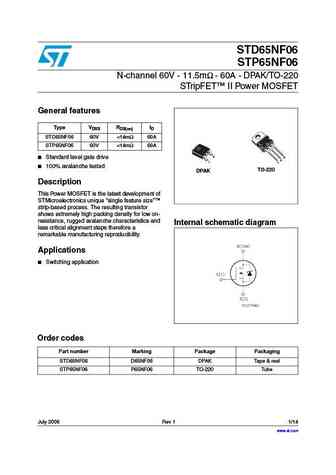
STD65NF06 STP65NF06 N-channel 60V - 11.5m - 60A - DPAK/TO-220 STripFET II Power MOSFET General features Type VDSS RDS(on) ID STD65NF06 60V ... See More ⇒
stp65nf06.pdf
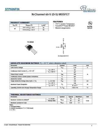
STP65NF06 www.VBsemi.tw N-Channel 60-V (D-S) MOSFET FEATURES PRODUCT SUMMARY 175 C Junction Temperature VDS (V) RDS(on) ( ) ID (A)a TrenchFET Power MOSFET 0.011 at VGS = 10 V 60 Material categorization 60 0.012 at VGS = 4.5 V 50 D TO-220AB G S D S G N-Channel MOSFET ABSOLUTE MAXIMUM RATINGS (TC = 25 C, unless otherwise noted) Parameter Symbol Limi... See More ⇒
stp65nf06.pdf
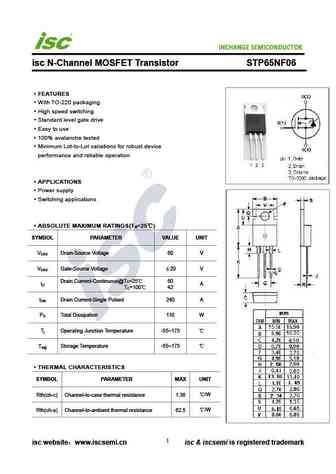
INCHANGE Semiconductor isc N-Channel MOSFET Transistor STP65NF06 FEATURES With TO-220 packaging High speed switching Standard level gate drive Easy to use 100% avalanche tested Minimum Lot-to-Lot variations for robust device performance and reliable operation APPLICATIONS Power supply Switching applications ABSOLUTE MAXIMUM RATINGS(T =25 ) a SYMBOL PARAMET... See More ⇒
stp652f.pdf
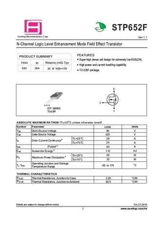
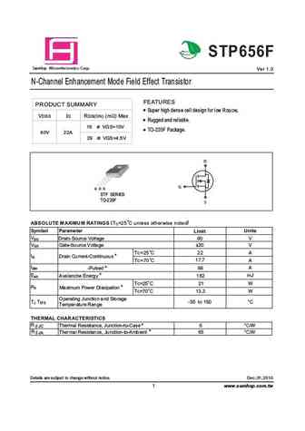
Gre r r P Pr Pr Pro STP652F a S mHop Microelectronics C orp. Ver 1.1 N-Channel Logic Level Enhancement Mode Field Effect Transistor FEATURES PRODUCT SUMMARY Super high dense cell design for extremely low RDS(ON). RDS(ON) (m ) Typ VDSS ID High power and current handling capability. 60V 29A 22 @ VGS=10V TO-220F package. D G G D S STF SERIES S TO-220F (TC=25 C unless ot... See More ⇒
Detailed specifications: STP60N55F3, STP60NF03L, STP60NF06, STP60NF06FP, STP60NF06L, STP60NF10, STP60NS04ZB, STP62NS04Z, IRFZ24N, STP6N120K3, STP6N52K3, STP6N62K3, STP6N95K5, STP6NK50Z, STP6NK60Z, STP6NK90Z, STP70N10F4
Keywords - STP65NF06 MOSFET specs
STP65NF06 cross reference
STP65NF06 equivalent finder
STP65NF06 pdf lookup
STP65NF06 substitution
STP65NF06 replacement
Step-by-step guide to finding a MOSFET replacement. Cross-reference parts and ensure compatibility for your repair or project.
MOSFET Parameters. How They Affect Each Other
🌐 : EN ES РУ

LIST
Last Update
MOSFET: CS95118 | CS85105A | CS75N45 | CS72N12 | CS55N50 | CS48N75A | CS40N27 | MSQ60P04D | MSQ40P07D | MSQ30P40D
Popular searches
d882 transistor equivalent | 17n80c3 | bc107 transistor | rjp63g4 datasheet | 2sc1115 | c3998 transistor | 2sa679 | 2sc3181