SPB03N60S5 Specs and Replacement
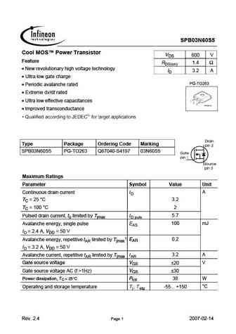
Type Designator: SPB03N60S5
Type of Transistor: MOSFET
Type of Control Channel: N-Channel
Absolute Maximum Ratings
Pd ⓘ - Maximum Power Dissipation: 38 W
|Vds|ⓘ - Maximum Drain-Source Voltage: 600 V
|Vgs|ⓘ - Maximum Gate-Source Voltage: 20 V
|Id| ⓘ - Maximum Drain Current: 3.2 A
Tj ⓘ - Maximum Junction Temperature: 150 °C
Electrical Characteristics
tr ⓘ - Rise Time: 25 nS
Cossⓘ - Output Capacitance: 150 pF
RDSonⓘ - Maximum Drain-Source On-State Resistance: 1.4 Ohm
Package: TO263
SPB03N60S5 substitution
- MOSFET ⓘ Cross-Reference Search
SPB03N60S5 datasheet
spb03n60s5.pdf
SPB03N60S5 Cool MOS Power Transistor VDS 600 V Feature RDS(on) 1.4 New revolutionary high voltage technology ID 3.2 A Ultra low gate charge PG-TO263 Periodic avalanche rated Extreme dv/dt rated Ultra low effective capacitances Improved transconductance Type Package Ordering Code Marking SPB03N60S5 PG-TO263 Q67040-S4197 03N60S5 Maximum Ratings Para... See More ⇒
spb03n60c3.pdf
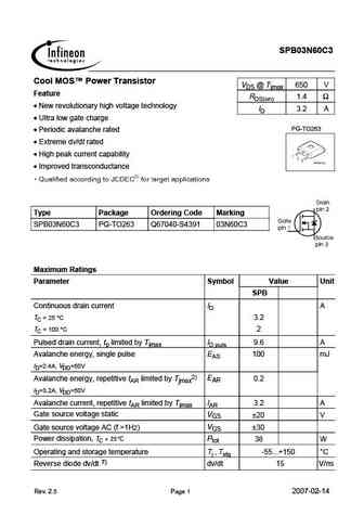
Isc N-Channel MOSFET Transistor SPB03N60C3 FEATURES With To-263(D2PAK) package Low input capacitance and gate charge Low gate input resistance 100% avalanche tested Minimum Lot-to-Lot variations for robust device performance and reliable operation APPLICATIONS Switching applications ABSOLUTE MAXIMUM RATINGS(T =25 ) a SYMBOL PARAMETER VALUE UNIT V Drain-Source Vo... See More ⇒
Detailed specifications: SPA20N60C3, SPA20N60CFD, SPA20N65C3, SPA21N50C3, SPB80N06S-08, SPB02N60C3, SPB02N60S5, SPB03N60C3, TK10A60D, SPB04N50C3, SPB04N60C3, SPB04N60S5, SPB07N60C3, SPB07N60S5, SPB08P06PG, SPB100N03S2-03G, SPB10N10LG
Keywords - SPB03N60S5 MOSFET specs
SPB03N60S5 cross reference
SPB03N60S5 equivalent finder
SPB03N60S5 pdf lookup
SPB03N60S5 substitution
SPB03N60S5 replacement
Learn how to find the right MOSFET substitute. A guide to cross-reference, check specs and replace MOSFETs in your circuits.
🌐 : EN ES РУ
LIST
Last Update
MOSFET: AUW033N08BG | AUW025N10 | AUR030N10 | AUR020N10 | AUR020N085 | AUR014N10 | AUP074N10 | AUP065N10 | AUP062N08BG | AUP060N08AG
Popular searches
tip130 | se9302 transistor | fr5305 datasheet | y2 transistor | 40n06 | bc108b | oc84 | c6090


