TK40A10N1 Specs and Replacement
Type Designator: TK40A10N1
Type of Transistor: MOSFET
Type of Control Channel: N-Channel
Absolute Maximum Ratings
Pd ⓘ - Maximum Power Dissipation: 35 W
|Vds|ⓘ - Maximum Drain-Source Voltage: 100 V
|Vgs|ⓘ - Maximum Gate-Source Voltage: 20 V
|Id| ⓘ - Maximum Drain Current: 40 A
Tj ⓘ - Maximum Junction Temperature: 150 °C
Electrical Characteristics
tr ⓘ - Rise Time: 14 nS
Cossⓘ - Output Capacitance: 520 pF
RDSonⓘ - Maximum Drain-Source On-State Resistance: 0.0082 Ohm
Package: TO220SIS
TK40A10N1 substitution
- MOSFET ⓘ Cross-Reference Search
TK40A10N1 datasheet
tk40a10n1.pdf
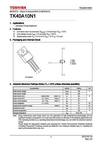
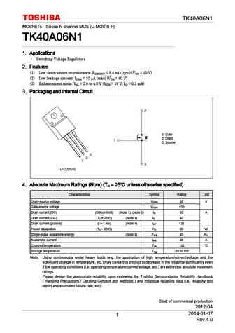
TK40A10N1 MOSFETs Silicon N-channel MOS (U-MOS -H) TK40A10N1 TK40A10N1 TK40A10N1 TK40A10N1 1. Applications 1. Applications 1. Applications 1. Applications Switching Voltage Regulators 2. Features 2. Features 2. Features 2. Features (1) Low drain-source on-resistance RDS(ON) = 6.8 m (typ.) (VGS = 10 V) (2) Low leakage current IDSS = 10 A (max) (VDS = 100 V) (3) Enha... See More ⇒
tk40a10n1.pdf
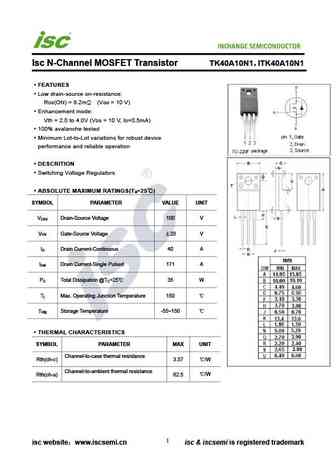
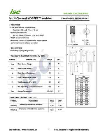
INCHANGE Semiconductor Isc N-Channel MOSFET Transistor TK40A10N1 ITK40A10N1 FEATURES Low drain-source on-resistance RDS(ON) = 8.2m (VGS = 10 V) Enhancement mode Vth = 2.0 to 4.0V (VDS = 10 V, ID=0.5mA) 100% avalanche tested Minimum Lot-to-Lot variations for robust device performance and reliable operation DESCRITION Switching Voltage Regulators ABSOLUTE MAXI... See More ⇒
tk40a10j1.pdf
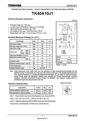
TK40A10J1 TOSHIBA Field Effect Transistor Silicon N Channel MOS Type (Ultra-High-Speed U-MOS ) TK40A10J1 Switching Regulator Applications Unit mm Small gate charge Qg = 76nC (typ.) Low drain-source ON-resistance RDS (ON) = 11.5 m (typ.) High forward transfer admittance Yfs = 90 S Low leakage current IDSS = 10 A (max) (VDS = 100 V) Enhancement m... See More ⇒
tk40a10k3.pdf
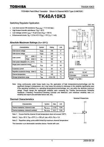
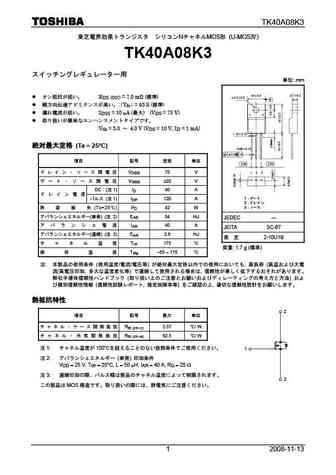
TK40A10K3 TOSHIBA Field Effect Transistor Silicon N Channel MOS Type (U-MOS ) TK40A10K3 Switching Regulator Application Unit mm Low drain-source ON resistance RDS (ON) = 11.5 m (typ.) High forward transfer admittance Yfs = 80 S Low leakage current IDSS = 10 A (max) (VDS = 100 V) Enhancement-mode Vth = 2.0 to 4.0 V (VDS = 10 V, ID = 1 mA) Absolute M... See More ⇒
Detailed specifications: TK17A25D, TK19H50C, TK20A20D, TK20A60T, TK20D60T, TK20D60U, TK20H50C, TK20J60T, SI2302, TK40D10J1, TK40E10N1, TK50F15J1, TK55D10J1, TK60D08J1, TK65A10N1, TK65E10N1, TK6B60D
Keywords - TK40A10N1 MOSFET specs
TK40A10N1 cross reference
TK40A10N1 equivalent finder
TK40A10N1 pdf lookup
TK40A10N1 substitution
TK40A10N1 replacement
Can't find your MOSFET? Learn how to find a substitute transistor by analyzing voltage, current and package compatibility
History: APT5024SLL
🌐 : EN ES РУ

LIST
Last Update
MOSFET: AUB062N08BG | AUB060N08AG | AUB056N10 | AUB056N08BGL | AUB050N085 | AUB050N055 | AUB045N12 | AUB045N10BT | AUB039N10 | AUB034N10
Popular searches
2n3904 transistor datasheet | p75nf75 | d880 transistor | 2sc1845 | p60nf06 | 2sa1837 | ksc1845 transistor | irf630 datasheet