FDB4020P Specs and Replacement
Type Designator: FDB4020P
Type of Transistor: MOSFET
Type of Control Channel: P-Channel
Absolute Maximum Ratings
Pd ⓘ - Maximum Power Dissipation: 37.5 W
|Vds|ⓘ - Maximum Drain-Source Voltage: 20 V
|Vgs|ⓘ - Maximum Gate-Source Voltage: 8 V
|Id| ⓘ - Maximum Drain Current: 16 A
Tj ⓘ - Maximum Junction Temperature: 175 °C
Electrical Characteristics
tr ⓘ - Rise Time: 24 nS
Cossⓘ - Output Capacitance: 270 pF
RDSonⓘ - Maximum Drain-Source On-State Resistance: 0.08 Ohm
Package: TO263AB
FDB4020P substitution
- MOSFET ⓘ Cross-Reference Search
FDB4020P datasheet
fdp4020p fdb4020p.pdf
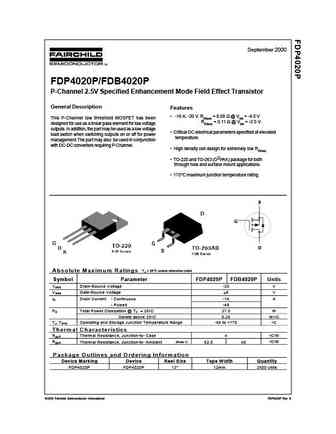
September 2000 FDP4020P/FDB4020P P-Channel 2.5V Specified Enhancement Mode Field Effect Transistor General Description Features -16 A, -20 V. RDS(on) = 0.08 @ VGS = -4.5 V This P-Channel low threshold MOSFET has been RDS(on) = 0.11 @ VGS = -2.5 V. designed for use as a linear pass element for low voltage outputs. In addition, the part may be used as a low voltage Criti... See More ⇒
fdp4030l fdb4030l.pdf
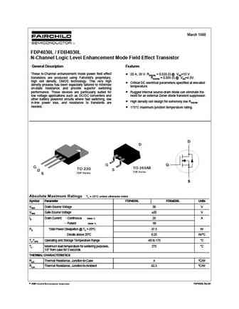
March 1998 FDP4030L / FDB4030L N-Channel Logic Level Enhancement Mode Field Effect Transistor General Description Features These N-Channel enhancement mode power field effect 20 A, 30 V. RDS(ON) = 0.035 @ VGS=10 V transistors are produced using Fairchild's proprietary, RDS(ON) = 0.055 @ VGS=4.5V. high cell density, DMOS technology. This very high Critical DC electrical parame... See More ⇒
Detailed specifications: F5032, F5033, F5038H, FA38SA50LC, FA57SA50LC, FB180SA10, AO3423B, AS2306, 2SK3878, FDB4030L, FDB5680, FDB5690, FDB6030BL, FDB6030L, FDB6035AL, FDB6035L, FDB603AL
Keywords - FDB4020P MOSFET specs
FDB4020P cross reference
FDB4020P equivalent finder
FDB4020P pdf lookup
FDB4020P substitution
FDB4020P replacement
Can't find your MOSFET? Learn how to find a substitute transistor by analyzing voltage, current and package compatibility
History: AO4498E
🌐 : EN ES РУ
LIST
Last Update
MOSFET: AUN084N10 | AUN065N10 | AUN063N10 | AUN062N08BG | AUN060N08AG | AUN053N10 | AUN050N08BGL | AUN045N085 | AUN042N055 | AUN036N10
Popular searches
2sb1186a | a1695 datasheet | 3415 transistor | 072ne6pt | 2sd388 | 2sc1400 | 2sd331 | 2sc1312 datasheet


