CEP1195 Datasheet. Specs and Replacement
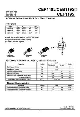
Type Designator: CEP1195 📄📄
Type of Transistor: MOSFET
Type of Control Channel: N-Channel
Absolute Maximum Ratings
Pd ⓘ - Maximum Power Dissipation: 166 W
|Vds|ⓘ - Maximum Drain-Source Voltage: 900 V
|Vgs|ⓘ - Maximum Gate-Source Voltage: 30 V
|Id| ⓘ - Maximum Drain Current: 5 A
Tj ⓘ - Maximum Junction Temperature: 150 °C
Electrical Characteristics
tr ⓘ - Rise Time: 21.5 nS
Cossⓘ - Output Capacitance: 130 pF
RDSonⓘ - Maximum Drain-Source On-State Resistance: 2.75 Ohm
Package: TO220
📄📄 Copy
CEP1195 substitution
- MOSFET ⓘ Cross-Reference Search
CEP1195 datasheet
cep1195 ceb1195 cef1195.pdf
CEP1195/CEB1195 CEF1195 N-Channel Enhancement Mode Field Effect Transistor FEATURES Type VDSS RDS(ON) ID @VGS CEP1195 900V 2.75 5A 10V CEB1195 900V 2.75 5A 10V CEF1195 900V 2.75 5A d 10V D Super high dense cell design for extremely low RDS(ON). High power and current handing capability. Lead free product is acquired. G S CEB SERIES CEP SERIES CEF SERIES TO-263(DD-PAK) ... See More ⇒
ceb110p03 cep110p03.pdf
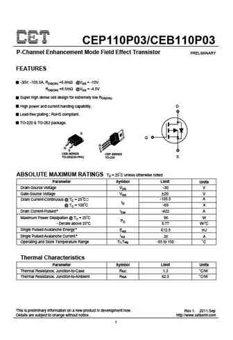
CEP110P03/CEB110P03 P-Channel Enhancement Mode Field Effect Transistor PRELIMINARY FEATURES -30V, -105.5A, RDS(ON) =5.8m @VGS = -10V. RDS(ON) =8.5m @VGS = -4.5V. Super high dense cell design for extremely low RDS(ON). High power and current handing capability. D Lead-free plating ; RoHS compliant. TO-220 & TO-263 package. G CEB SERIES CEP SERIES TO-263(DD-PAK) S TO-220 ABS... See More ⇒
cep1186 ceb1186 cef1186.pdf
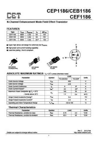
CEP1186/CEB1186 CEF1186 N-Channel Enhancement Mode Field Effect Transistor FEATURES Type VDSS RDS(ON) ID @VGS CEP1186 800V 2.3 6A 10V CEB1186 800V 2.3 6A 10V CEF1186 800V 2.3 6A d 10V D Super high dense cell design for extremely low RDS(ON). High power and current handing capability. Lead-free plating ; RoHS compliant. G S CEB SERIES CEP SERIES CEF SERIES TO-263(DD-PAK)... See More ⇒
ncep11n10as.pdf
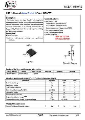
NCEP11N10AS NCE N-Channel Super Trench II Power MOSFET Description General Features The series of devices uses Super Trench II technology that is VDS =100V,ID =12A uniquely optimized to provide the most efficient high frequency RDS(ON)=9.1m , typical@ VGS=10V switching performance. Both conduction and switching power RDS(ON)=12m , typical@ VGS=4.5V losses are minim... See More ⇒
Detailed specifications: CEB08N6A, CEF08N6A, CEP08N6A, CEF1186, CEB1186, CEP1186, CEB1195, CEF1195, IRF840, CEB21A2, CEB3060, CEB30N15L, CEB3120, CEB3205, CEB4060A, CEB4060AL, CEB45N10
Keywords - CEP1195 MOSFET specs
CEP1195 cross reference
CEP1195 equivalent finder
CEP1195 pdf lookup
CEP1195 substitution
CEP1195 replacement
Can't find your MOSFET? Learn how to find a substitute transistor by analyzing voltage, current and package compatibility
MOSFET Parameters. How They Affect Each Other
History: G3205 | JMSH1102QE | APG060N85D | IPD70N03S4L-04 | ME2328-G | PSMN5R2-60YL | CS20N60F
🌐 : EN ES РУ
LIST
Last Update
MOSFET: CS95118 | CS85105A | CS75N45 | CS72N12 | CS55N50 | CS48N75A | CS40N27 | MSQ60P04D | MSQ40P07D | MSQ30P40D
Popular searches
mj15023 | tip36c transistor | 2sc3320 | 2sc2078 | ac127 transistor | a42 transistor | bc547c | 2sa726
