CED40N10 Specs and Replacement
Type Designator: CED40N10
Type of Transistor: MOSFET
Type of Control Channel: N-Channel
Absolute Maximum Ratings
Pd ⓘ - Maximum Power Dissipation: 93.8 W
|Vds|ⓘ - Maximum Drain-Source Voltage: 100 V
|Vgs|ⓘ - Maximum Gate-Source Voltage: 20 V
|Id| ⓘ - Maximum Drain Current: 37 A
Tj ⓘ - Maximum Junction Temperature: 175 °C
Electrical Characteristics
tr ⓘ - Rise Time: 30 nS
Cossⓘ - Output Capacitance: 330 pF
RDSonⓘ - Maximum Drain-Source On-State Resistance: 0.032 Ohm
Package: TO251
CED40N10 substitution
- MOSFET ⓘ Cross-Reference Search
CED40N10 datasheet
ceu40n10 ced40n10.pdf
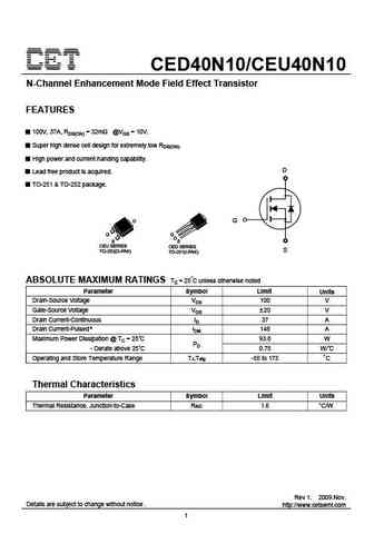
CED40N10/CEU40N10 N-Channel Enhancement Mode Field Effect Transistor FEATURES 100V, 37A, RDS(ON) = 32m @VGS = 10V. Super high dense cell design for extremely low RDS(ON). High power and current handing capability. D Lead free product is acquired. TO-251 & TO-252 package. D G G S CEU SERIES CED SERIES S TO-252(D-PAK) TO-251(I-PAK) ABSOLUTE MAXIMUM RATINGS Tc = 25 C unless oth... See More ⇒
ceu4060al ced4060al.pdf

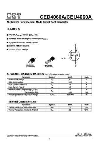
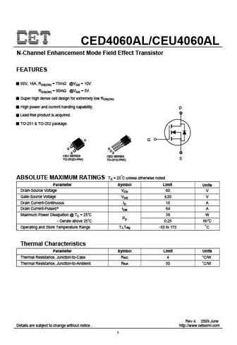
CED4060AL/CEU4060AL N-Channel Enhancement Mode Field Effect Transistor FEATURES 60V, 16A, RDS(ON) = 75m @VGS = 10V. RDS(ON) = 90m @VGS = 5V. Super high dense cell design for extremely low RDS(ON). High power and current handing capability. D Lead free product is acquired. TO-251 & TO-252 package. D G G S CEU SERIES CED SERIES S TO-252(D-PAK) TO-251(I-PAK) ABSOLUTE MAXIM... See More ⇒
ced4060a ceu4060a.pdf

CED4060A/CEU4060A N-Channel Enhancement Mode Field Effect Transistor FEATURES 60V, 15A, RDS(ON) = 85m @VGS = 10V. Super high dense cell design for extremely low RDS(ON). High power and current handing capability. D Lead free product is acquired. TO-251 & TO-252 package. D G G S CEU SERIES CED SERIES S TO-252(D-PAK) TO-251(I-PAK) ABSOLUTE MAXIMUM RATINGS Tc = 25 C unless othe... See More ⇒
ceu4060a ced4060a.pdf
CED4060A/CEU4060A N-Channel Enhancement Mode Field Effect Transistor FEATURES 60V, 15A, RDS(ON) = 85m @VGS = 10V. Super high dense cell design for extremely low RDS(ON). High power and current handing capability. D Lead free product is acquired. TO-251 & TO-252 package. D G G S CEU SERIES CED SERIES S TO-252(D-PAK) TO-251(I-PAK) ABSOLUTE MAXIMUM RATINGS Tc = 25 C unless othe... See More ⇒
Detailed specifications: CED25N15L, CED3060, CED3100, CED3120, CED3172, CED3252, CED4060A, CED4060AL, 4N60, CED4204, CED540L, CED540N, CED55N10, CED6056, CED6060N, CED6086, CED6186
Keywords - CED40N10 MOSFET specs
CED40N10 cross reference
CED40N10 equivalent finder
CED40N10 pdf lookup
CED40N10 substitution
CED40N10 replacement
Step-by-step guide to finding a MOSFET replacement. Cross-reference parts and ensure compatibility for your repair or project.
🌐 : EN ES РУ

LIST
Last Update
MOSFET: AKF30N5P0SX | AKF30N10S | AKF20P45D | CM4407 | CM3407 | CM3400 | SVF11N65F | SVF11N65T | FKBB3105 | EHBA036R1
Popular searches
2sc2362 | 2sd468 | c2240 transistor | 2sc1918 | c1213 transistor | 2sc1400 replacement | 2sb817 | mn2488 datasheet