2N5460 Specs and Replacement
Type Designator: 2N5460
Type of Transistor: JFET
Type of Control Channel: P-Channel
Absolute Maximum Ratings
Pd ⓘ
- Maximum Power Dissipation: 0.35 W
|Vds|ⓘ - Maximum Drain-Source Voltage: 40 V
|Vgs|ⓘ - Maximum Gate-Source Voltage: 4 V
|Id| ⓘ - Maximum Drain Current: 0.005 A
Tj ⓘ - Maximum Junction Temperature: 150 °C
Electrical Characteristics
Package: TO-92
- MOSFET ⓘ Cross-Reference Search
2N5460 datasheet
..2. Size:114K fairchild semi
2n5460 2n5461 2n5462 mmbf5460 mmbf5461 mmbf5462.pdf 
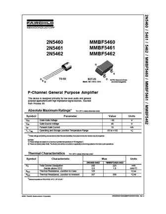
2N5460 MMBF5460 2N5461 MMBF5461 2N5462 MMBF5462 G S G TO-92 D SOT-23 NOTE Source & Drain S Mark 6E / 61U / 61V are interchangeable D P-Channel General Purpose Amplifier This device is designed primarily for low level audio and general purpose applications with high impedance signal sources. Sourced from Process 89. Absolute Maximum Ratings* TA = 25 C unless otherwise noted - ... See More ⇒
..3. Size:48K vishay
2n5460 sst5460 2n5461 sst5461 2n5462 sst5462.pdf
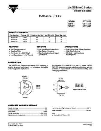
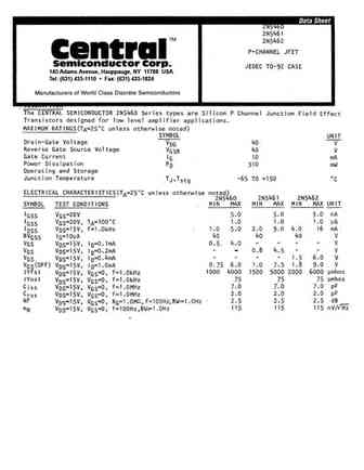
2N/SST5460 Series Vishay Siliconix P-Channel JFETs 2N5460 SST5460 2N5461 SST5461 2N5462 SST5462 PRODUCT SUMMARY Part Number VGS(off) (V) V(BR)GSS Min (V) gfs Min (mS) IDSS Min (mA) 2N/SST5460 0.75 to 6 40 1 1 2N/SST5461 1 to 7.5 40 1.5 2 2N/SST5462 1.8 to 9 40 2 4 FEATURES BENEFITS APPLICATIONS D High Input Impedance D Low Signal Loss/System Error D Low-Current, Low-Voltage... See More ⇒
..5. Size:60K onsemi
2n5460 2n5461 2n5462.pdf
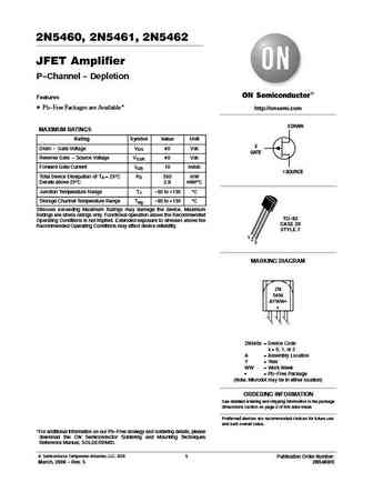
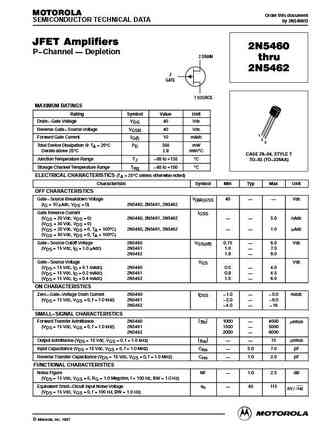
2N5460, 2N5461, 2N5462 JFET Amplifier P-Channel - Depletion Features Pb-Free Packages are Available* http //onsemi.com 2 DRAIN MAXIMUM RATINGS Rating Symbol Value Unit 3 Drain - Gate Voltage VDG 40 Vdc GATE Reverse Gate - Source Voltage VGSR 40 Vdc Forward Gate Current IG(f) 10 mAdc 1 SOURCE Total Device Dissipation @ TA = 25 C PD 350 mW Derate above 25 C 2.8 mW/ C Junct... See More ⇒
9.1. Size:11K semelab
2n5468.pdf
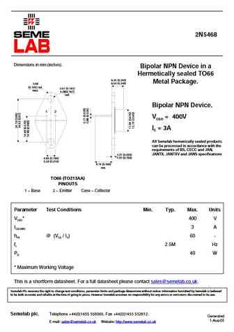
2N5468 Dimensions in mm (inches). Bipolar NPN Device in a Hermetically sealed TO66 6.35 (0.250) Metal Package. 8.64 (0.340) 3.68 (0.145) rad. 3.61 (0.142) max. 4.08(0.161) rad. Bipolar NPN Device. 1 2 VCEO = 400V IC = 3A All Semelab hermetically sealed products can be processed in accordance with the requirements of BS, CECC and JAN, JANTX, JANTXV and JANS speci... See More ⇒
9.2. Size:11K semelab
2n5469.pdf

2N5469 Dimensions in mm (inches). Bipolar NPN Device in a Hermetically sealed TO66 6.35 (0.250) Metal Package. 8.64 (0.340) 3.68 (0.145) rad. 3.61 (0.142) max. 4.08(0.161) rad. Bipolar NPN Device. 1 2 VCEO = 400V IC = 3A All Semelab hermetically sealed products can be processed in accordance with the requirements of BS, CECC and JAN, JANTX, JANTXV and JANS speci... See More ⇒
9.3. Size:11K semelab
2n5467.pdf
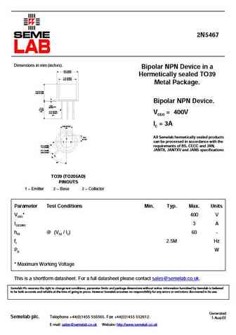
2N5467 Dimensions in mm (inches). Bipolar NPN Device in a 8.51 (0.34) 9.40 (0.37) Hermetically sealed TO39 7.75 (0.305) 8.51 (0.335) Metal Package. 6.10 (0.240) 6.60 (0.260) Bipolar NPN Device. 0.89 max. (0.035) 12.70 (0.500) min. 0.41 (0.016) 0.53 (0.021) VCEO = 400V dia. IC = 3A 5.08 (0.200) typ. 2.54 All Semelab hermetically sealed products 2 (0.100) 1 3... See More ⇒
9.4. Size:184K inchange semiconductor
2n5468.pdf
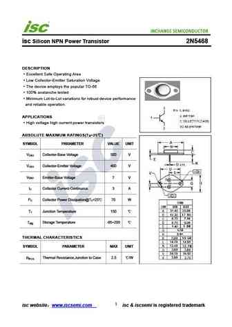
isc Silicon NPN Power Transistor 2N5468 DESCRIPTION Excellent Safe Operating Area Low Collector-Emitter Saturation Voltage The device employs the popular TO-66 100% avalanche tested Minimum Lot-to-Lot variations for robust device performance and reliable operation. APPLICATIONS High voltage high current power transistors ABSOLUTE MAXIMUM RATINGS(T =25 ) a SYMBOL PARAME... See More ⇒
9.5. Size:184K inchange semiconductor
2n5469.pdf

isc Silicon NPN Power Transistor 2N5469 DESCRIPTION Excellent Safe Operating Area Low Collector-Emitter Saturation Voltage The device employs the popular TO-66 100% avalanche tested Minimum Lot-to-Lot variations for robust device performance and reliable operation. APPLICATIONS High voltage high current power transistors ABSOLUTE MAXIMUM RATINGS(T =25 ) a SYMBOL PARAME... See More ⇒
9.6. Size:129K inchange semiconductor
2n5468 2n5469.pdf
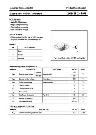
Inchange Semiconductor Product Specification Silicon NPN Power Transistors 2N5468 2N5469 DESCRIPTION With TO-66 package High-voltage capability Fast switching speeds Low saturation voltage APPLICATIONS They are intended for use in off-line power supplies ,inverter and converter circuits PINNING PIN DESCRIPTION 1 Base 2 Emitter Fig.1 simplified outline (TO-66)... See More ⇒
9.7. Size:130K inchange semiconductor
2n5466 2n5467.pdf
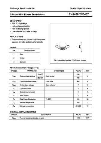
Inchange Semiconductor Product Specification Silicon NPN Power Transistors 2N5466 2N5467 DESCRIPTION With TO-3 package High-voltage capability Fast switching speeds Low collector saturation voltage APPLICATIONS They are intended for use in off-line power supplies ,inverter and converter circuits PINNING PIN DESCRIPTION 1 Base 2 Emitter Fig.1 simplified outlin... See More ⇒
9.8. Size:182K inchange semiconductor
2n5467.pdf
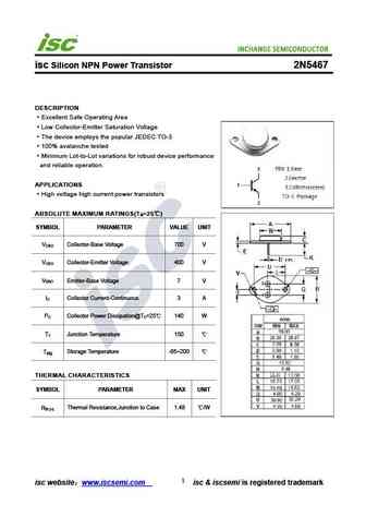
isc Silicon NPN Power Transistor 2N5467 DESCRIPTION Excellent Safe Operating Area Low Collector-Emitter Saturation Voltage The device employs the popular JEDEC TO-3 100% avalanche tested Minimum Lot-to-Lot variations for robust device performance and reliable operation. APPLICATIONS High voltage high current power transistors ABSOLUTE MAXIMUM RATINGS(T =25 ) a SYMBOL P... See More ⇒
9.9. Size:182K inchange semiconductor
2n5466.pdf
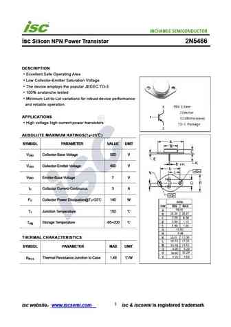
isc Silicon NPN Power Transistor 2N5466 DESCRIPTION Excellent Safe Operating Area Low Collector-Emitter Saturation Voltage The device employs the popular JEDEC TO-3 100% avalanche tested Minimum Lot-to-Lot variations for robust device performance and reliable operation. APPLICATIONS High voltage high current power transistors ABSOLUTE MAXIMUM RATINGS(T =25 ) a SYMBOL P... See More ⇒
Detailed specifications: 2N5433
, 2N5434
, 2N5452
, 2N5453
, 2N5454
, 2N5457
, 2N5458
, 2N5459
, IRF9540
, 2N5461
, 2N5462
, 2N5515
, 2N5516
, 2N5517
, 2N5518
, 2N5519
, 2N5520
.
Keywords - 2N5460 MOSFET specs
2N5460 cross reference
2N5460 equivalent finder
2N5460 pdf lookup
2N5460 substitution
2N5460 replacement
Learn how to find the right MOSFET substitute. A guide to cross-reference, check specs and replace MOSFETs in your circuits.