J270 Specs and Replacement
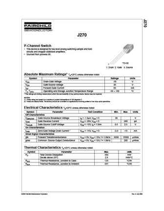
Type Designator: J270
Type of Transistor: JFET
Type of Control Channel: P-Channel
Absolute Maximum Ratings
Pd ⓘ - Maximum Power Dissipation: 0.35 W
|Vds|ⓘ - Maximum Drain-Source Voltage: 30 V
|Vgs|ⓘ - Maximum Gate-Source Voltage: 2 V
|Id| ⓘ - Maximum Drain Current: 0.015 A
Tj ⓘ - Maximum Junction Temperature: 150 °C
Electrical Characteristics
RDSonⓘ - Maximum Drain-Source On-State Resistance: 200 Ohm
Package: TO-92
J270 substitution
- MOSFET ⓘ Cross-Reference Search
J270 datasheet
j270.pdf
J270 P-Channel Switch This device is designed for low level analog switching sample and hold circuits and chopper stabilized amplifiers. Sourced from process 88. TO-92 1 1. Drain 2. Gate 3. Source Absolute Maximum Ratings* Ta=25 C unless otherwise noted Symbol Parameter Ratings Units VDG Drain-Gate Voltage -30 V VGS Gate-Source Voltage 30 V IGF Forward Gate Current 50 mA ... See More ⇒
j270 sst270 j271 sst271.pdf
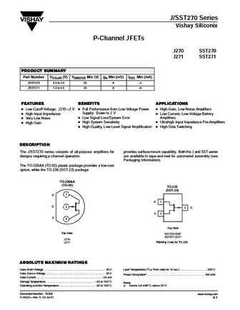
J/SST270 Series Vishay Siliconix P-Channel JFETs J270 SST270 J271 SST271 PRODUCT SUMMARY Part Number VGS(off) (V) V(BR)GSS Min (V) gfs Min (mS) IDSS Min (mA) J/SST270 0.5 to 2.0 30 6 2 J/SST271 1.5 to 4.5 30 8 6 FEATURES BENEFITS APPLICATIONS D Low Cutoff Voltage J270 ... See More ⇒
j270 j271 sst270 sst271.pdf
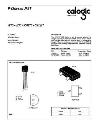
P-Channel JFET CORPORATION J270 J271 / SST270 SST271 FEATURES DESCRIPTION Surface Mount The J270/SST270 Series is an all-purpose amplifier for designs requiring P-channel operation. These devices feature APPLICATIONS high gain, low noise and tight V limits for simple circuit GS(OFF) design. They are available in low-cost SOT-23 and TO-92 P-Channel Amplifier p... See More ⇒
mmbfj270.pdf
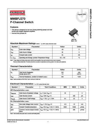
August 2008 MMBFJ270 P-Channel Switch Features This device is designed for low level analog switching sample and hold G circuits and chopper stabilized amplifiers. Sourced from process 88. S D SOT-23 Mark 61S Absolute Maximum Ratings (Note1) Ta = 25 C unless otherwise noted Symbol Parameter Value Units VDG Drain-Gate Voltage -30 V VGS Gate-Source Voltage 30 V IGF Fo... See More ⇒
Detailed specifications: J201 , J202 , MMBFJ201 , MMBFJ202 , J210 , MMBFJ210 , MMBFJ211 , MMBFJ212 , IRF640 , J271 , J304 , J305 , KSK30 , KSK595H , KSK596 , LS4117 , LS4118 .
History: J271
Keywords - J270 MOSFET specs
J270 cross reference
J270 equivalent finder
J270 pdf lookup
J270 substitution
J270 replacement
Can't find your MOSFET? Learn how to find a substitute transistor by analyzing voltage, current and package compatibility
History: J271
🌐 : EN ES РУ
LIST
Last Update
MOSFET: ASD80R750E | ASD70R950E | ASD70R600E | ASD70R380E | ASD65R850E | ASD65R550E | ASD65R350E | ASD65R300E | ASD65R280E | ASD65R270E
Popular searches
irf740 | c945 transistor | irf640n | 2n3904 | bc547 datasheet | k3797 mosfet | bs170 datasheet | tip41c
