MPF102 Specs and Replacement
Type Designator: MPF102
Type of Transistor: JFET
Type of Control Channel: N-Channel
Absolute Maximum Ratings
Pd ⓘ - Maximum Power Dissipation: 0.35 W
|Vds|ⓘ - Maximum Drain-Source Voltage: 25 V
|Vgs|ⓘ - Maximum Gate-Source Voltage: 7.5 V
|Id| ⓘ - Maximum Drain Current: 0.02 A
Tj ⓘ - Maximum Junction Temperature: 155 °C
Electrical Characteristics
Package: TO-92
MPF102 substitution
- MOSFET ⓘ Cross-Reference Search
MPF102 datasheet
mpf102.pdf
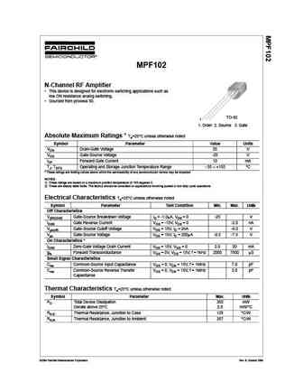
MPF102 N-Channel RF Amplifier This device is designed for electronic switching applications such as low ON resistance analog switching. Sourced from process 50. TO-92 1 1. Drain 2. Source 3. Gate Absolute Maximum Ratings * Ta=25 C unless otherwise noted Symbol Parameter Value Units VDG Drain-Gate Voltage 25 V VGS Gate-Source Voltage -25 V IGF Forward Gate Current 10 mA TJ... See More ⇒
mpf102.pdf
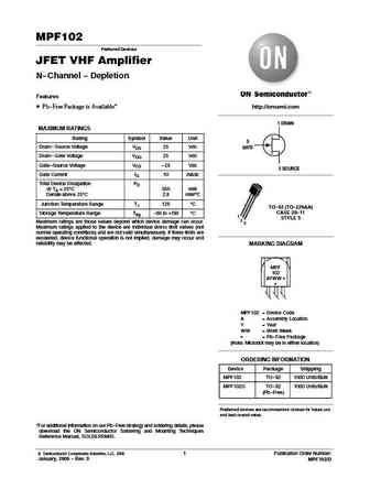
MPF102 Preferred Devices JFET VHF Amplifier N-Channel - Depletion Features Pb-Free Package is Available* http //onsemi.com 1 DRAIN MAXIMUM RATINGS Rating Symbol Value Unit 3 Drain-Source Voltage VDS 25 Vdc GATE Drain-Gate Voltage VDG 25 Vdc Gate-Source Voltage VGS -25 Vdc 2 SOURCE Gate Current IG 10 mAdc Total Device Dissipation PD @ TA = 25 C 350 mW Derate above 25 C 2... See More ⇒
mpf102rev0d.pdf
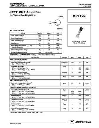
MOTOROLA Order this document SEMICONDUCTOR TECHNICAL DATA by MPF102/D JFET VHF Amplifier N Channel Depletion MPF102 1 DRAIN 3 GATE 2 SOURCE MAXIMUM RATINGS Rating Symbol Value Unit Drain Source Voltage VDS 25 Vdc 1 2 3 Drain Gate Voltage VDG 25 Vdc Gate Source Voltage VGS 25 Vdc CASE 29 04, STYLE 5 Gate Current IG 10 mAdc TO 92 (TO 226AA) Total Device D... See More ⇒
tmp10n80 tmpf10n80.pdf
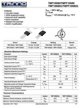
TMP10N80/TMPF10N80 TMP10N80G/TMPF10N80G VDSS = 880 V @Tjmax Features ID = 9.5A Low gate charge RDS(ON) = 1.05 W(max) @ VGS= 10 V 100% avalanche tested Improved dv/dt capability RoHS compliant Halogen free package JEDEC Qualification D G S Device Package Marking Remark TMP10N80 / TMPF10N80 TO-220 / TO-220F TMP10N80 / TMPF10N80 RoHS TMP10N... See More ⇒
Detailed specifications: MMBF5484 , MMBF5485 , MMBF5486 , MMBFJ270 , MMBFJ271 , J309 , MMBFJ309 , MMBFJ310 , IRF530 , P1086 , P1087 , STP11NB40 , STP11NB40FP , STP9NB50 , STP9NB50FP , PF5102 , PF5103 .
History: FDD6030BL
Keywords - MPF102 MOSFET specs
MPF102 cross reference
MPF102 equivalent finder
MPF102 pdf lookup
MPF102 substitution
MPF102 replacement
Can't find your MOSFET? Learn how to find a substitute transistor by analyzing voltage, current and package compatibility
History: FDD6030BL
🌐 : EN ES РУ

LIST
Last Update
MOSFET: ASA60R150E | ASA60R090EFDA | ASA60R090EFD | ASA50R130E | ADW120N080G2 | ADQ120N080G2 | ADG120N080G2 | AS6004 | 2N7002EY | AS2310A
Popular searches
tip3055 | mosfet datasheet | irf3205 datasheet | irf5210 | mj15024 | 2n2219 | tip42c | 2sc2240