7N90 Datasheet. Specs and Replacement
Type Designator: 7N90 📄📄
Type of Transistor: MOSFET
Type of Control Channel: N-Channel
Absolute Maximum Ratings
Pd ⓘ - Maximum Power Dissipation: 240 W
|Vds|ⓘ - Maximum Drain-Source Voltage: 900 V
|Vgs|ⓘ - Maximum Gate-Source Voltage: 30 V
|Id| ⓘ - Maximum Drain Current: 7 A
Tj ⓘ - Maximum Junction Temperature: 150 °C
Electrical Characteristics
tr ⓘ - Rise Time: 80 nS
Cossⓘ - Output Capacitance: 140 pF
RDSonⓘ - Maximum Drain-Source On-State Resistance: 1.5 Ohm
Package: TO-3P
TO-220F1
TO-220
TO-262
📄📄 Copy
- MOSFET ⓘ Cross-Reference Search
7N90 datasheet
..1. Size:187K utc
7n90.pdf 
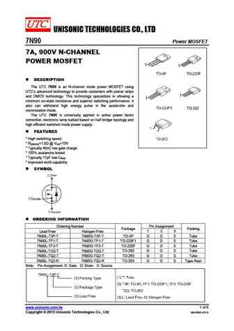
UNISONIC TECHNOLOGIES CO., LTD 7N90 Power MOSFET 7A, 900V N-CHANNEL POWER MOSFET DESCRIPTION The UTC 7N90 is an N-channel mode power MOSFET using UTC s advanced technology to provide costumers with planar stripe and DMOS technology. This technology specializes in allowing a minimum on-state resistance and superior switching performance. It also can withstand high energy puls... See More ⇒
0.3. Size:270K st
stf7n90k5.pdf
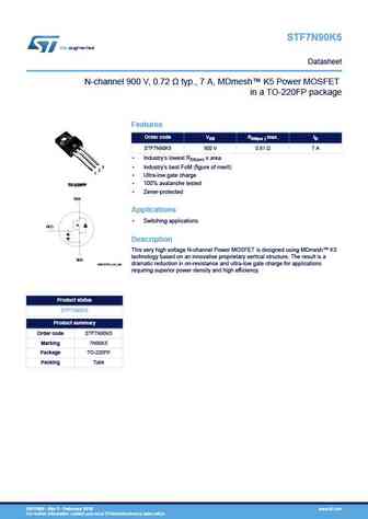
STF7N90K5 Datasheet N-channel 900 V, 0.72 typ., 7 A, MDmesh K5 Power MOSFET in a TO-220FP package Features Order code VDS RDS(on ) max. ID STF7N90K5 900 V 0.81 7 A Industry s lowest RDS(on) x area 3 Industry s best FoM (figure of merit) 2 1 Ultra-low gate charge 100% avalanche tested TO-220FP Zener-protected D(2) Applications Switching appl... See More ⇒
0.4. Size:681K fairchild semi
fqaf7n90.pdf
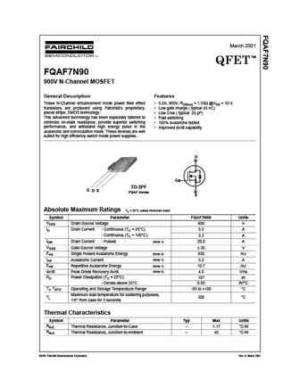
March 2001 TM QFET FQAF7N90 900V N-Channel MOSFET General Description Features These N-Channel enhancement mode power field effect 5.2A, 900V, RDS(on) = 1.55 @VGS = 10 V transistors are produced using Fairchild s proprietary, Low gate charge ( typical 45 nC) planar stripe, DMOS technology. Low Crss ( typical 20 pF) This advanced technology has been especially tailored... See More ⇒
0.5. Size:674K fairchild semi
fqa7n90.pdf

March 2001 TM QFET FQA7N90 900V N-Channel MOSFET General Description Features These N-Channel enhancement mode power field effect 7.4A, 900V, RDS(on) = 1.55 @VGS = 10 V transistors are produced using Fairchild s proprietary, Low gate charge ( typical 45 nC) planar stripe, DMOS technology. Low Crss ( typical 20 pF) This advanced technology has been especially tailored ... See More ⇒
0.6. Size:677K fairchild semi
fqa7n90m.pdf
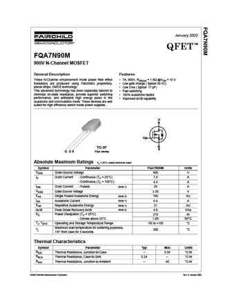
January 2002 TM QFET FQA7N90M 900V N-Channel MOSFET General Description Features These N-Channel enhancement mode power field effect 7A, 900V, RDS(on) = 1.8 @VGS = 10 V transistors are produced using Fairchild s proprietary, Low gate charge ( typical 40 nC) planar stripe, DMOS technology. Low Crss ( typical 17 pF) This advanced technology has been especially tailored ... See More ⇒
0.7. Size:928K samsung
ssf7n90a.pdf
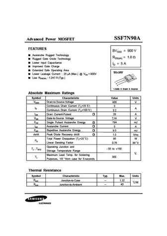
Advanced Power MOSFET FEATURES BVDSS = 900 V Avalanche Rugged Technology RDS(on) = 1.8 Rugged Gate Oxide Technology Lower Input Capacitance ID = 5 A Improved Gate Charge Extended Safe Operating Area Lower Leakage Current 25 A (Max.) @ VDS = 900V Low RDS(ON) 1.247 (Typ.) 1 2 3 1.Gate 2. Drain 3. Source Absolute Maximum Ratings Symbol Characteristic Value Un... See More ⇒
0.8. Size:930K samsung
ssh7n90a.pdf
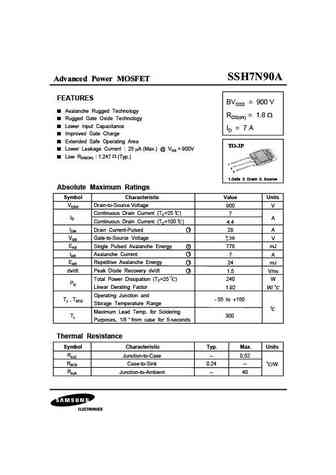
Advanced Power MOSFET FEATURES BVDSS = 900 V Avalanche Rugged Technology RDS(on) = 1.8 Rugged Gate Oxide Technology Lower Input Capacitance ID = 7 A Improved Gate Charge Extended Safe Operating Area Lower Leakage Current 25 A (Max.) @ VDS = 900V Low RDS(ON) 1.247 (Typ.) 1 2 3 1.Gate 2. Drain 3. Source Absolute Maximum Ratings Symbol Characteristic Value Un... See More ⇒
0.9. Size:112K ixys
ixfh7n90q ixft7n90q.pdf
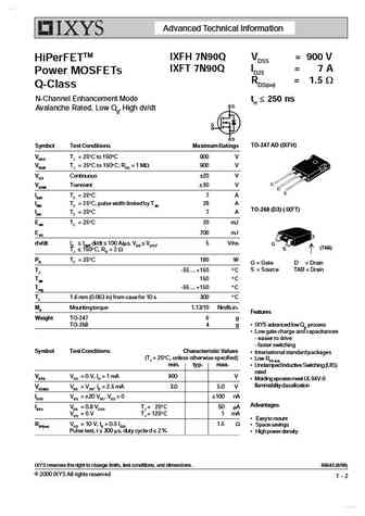
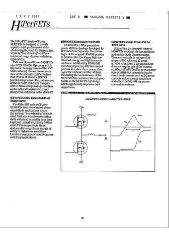
www.DataSheet.co.kr Advanced Technical Information IXFH 7N90Q VDSS = 900 V HiPerFETTM IXFT 7N90Q ID25 = 7 A Power MOSFETs RDS(on) = 1.5 W Q-Class N-Channel Enhancement Mode trr 250 ns Avalanche Rated, Low Qg, High dv/dt TO-247 AD (IXFH) Symbol Test Conditions Maximum Ratings VDSS TJ = 25 C to 150 C 900 V VDGR TJ = 25 C to 150 C; RGS = 1 MW 900 V VGS Continuous 20 V VGSM... See More ⇒
0.10. Size:346K fuji
fmh07n90e.pdf
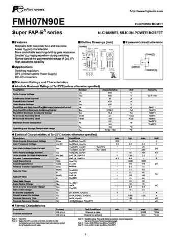
http //www.fujisemi.com FMH07N90E FUJI POWER MOSFET Super FAP-E3 series N-CHANNEL SILICON POWER MOSFET Features Outline Drawings [mm] Equivalent circuit schematic Maintains both low power loss and low noise TO-3P(Q) Lower R (on) characteristic DS More controllable switching dv/dt by gate resistance Drain(D) Smaller V ringing waveform during switching GS Narrow band of the gate thres... See More ⇒
0.11. Size:400K taiwansemi
tsm7n90ci tsm7n90cz.pdf
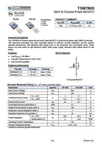
TSM7N90 900V N-Channel Power MOSFET TO-220 ITO-220 PRODUCT SUMMARY Pin Definition 1. Gate VDS (V) RDS(on)( ) ID (A) 2. Drain 3. Source 900 1.9 @ VGS =10V 3.5 General Description The TSM7N90 N-Channel enhancement mode Power MOSFET is produced by planar stripe DMOS technology. This advanced technology has been especially tailored to minimize on-state resistance, provi... See More ⇒
0.12. Size:369K nell
7n90a 7n90af.pdf
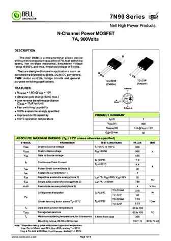
RoHS 7N90 Series RoHS SEMICONDUCTOR Nell High Power Products N-Channel Power MOSFET 7A, 900Volts DESCRIPTION D The Nell 7N90 is a three-terminal silicon device with current conduction capability of 7A, fast switching speed, low on-state resistance, breakdown voltage rating of 900V, and max. threshold voltage of 5 volts. They are designed for use in applications such as G G s... See More ⇒
0.13. Size:566K jiaensemi
jfpc7n90c jffm7n90c.pdf
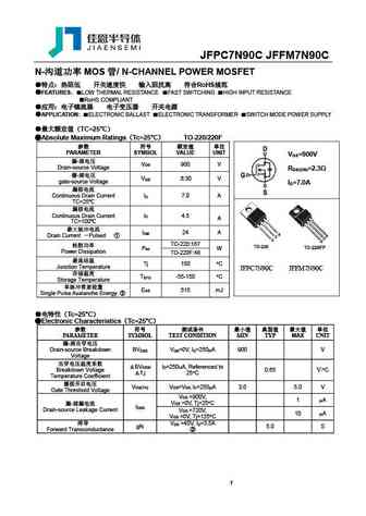
JFPC7N90C JFFM7N90C N- MOS / N-CHANNEL POWER MOSFET RoHS FEATURES LOW THERMAL RESISTANCE FAST SWITCHING HIGH INPUT RESISTANCE RoHS COMPLIANT APPLICATION ELECTRONIC BALLAST ELECTRONIC TRANSFORMER SWITCH MODE POWER SU... See More ⇒
0.14. Size:1165K jiaensemi
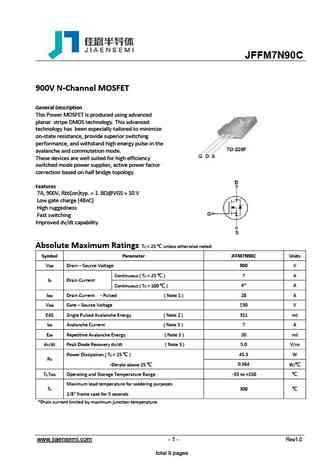
jfam7n90c.pdf

JFAM7N90C 900V N-Channel MOSFET General Description This Power MOSFET is produced using advanced planar stripe DMOS technology. This advanced technology has been especially tailored to minimize on-state resistance, provide superior switching performance, and withstand high energy pulse in the avalanche and commutation mode. These devices are well suited for high efficiency s... See More ⇒
0.15. Size:982K jiaensemi
jffm7n90c.pdf
JFFM7N90C 900V N-Channel MOSFET General Description This Power MOSFET is produced using advanced planar stripe DMOS technology. This advanced technology has been especially tailored to minimize on-state resistance, provide superior switching performance, and withstand high energy pulse in the avalanche and commutation mode. These devices are well suited for high efficiency s... See More ⇒
0.16. Size:750K samwin
swwf7n90d swmn7n90d.pdf
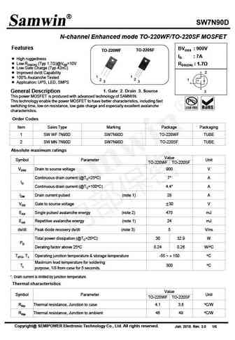
SW7N90D N-channel Enhanced mode TO-220WF/TO-220SF MOSFET Features BVDSS 900V TO-220WF TO-220SF ID 7A High ruggedness Low RDS(ON) (Typ 1.7 )@VGS=10V RDS(ON) 1.7 Low Gate Charge (Typ 42nC) 2 Improved dv/dt Capability 1 1 100% Avalanche Tested 2 2 1 3 3 Application UPS, LED, SMPS 1. Gate 2. Drain 3. Source General Descript... See More ⇒
0.17. Size:487K trinnotech
tma7n90 tman7n90.pdf
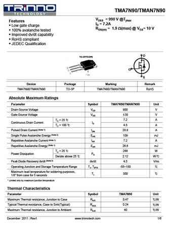
TMA7N90/TMAN7N90 VDSS = 990 V @Tjmax Features ID = 7.2A Low gate charge RDS(on) = 1.9 W(max) @ VGS= 10 V 100% avalanche tested Improved dv/dt capability RoHS compliant JEDEC Qualification D TO-3P/TO3PN G S Device Package Marking Remark TMA7N90/TMAN7N90 TO-3P TMA7N90/TMAN7N90 RoHS Absolute Maximum Ratings Parameter Symbol TMA7N90/TMAN7N90 Uni... See More ⇒
0.18. Size:440K trinnotech
tmp7n90 tmpf7n90.pdf
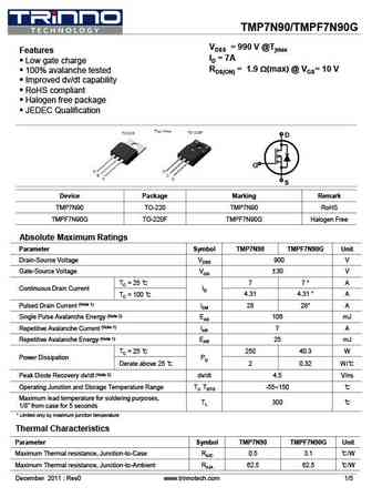
TMP7N90/TMPF7N90G VDSS = 990 V @Tjmax Features ID = 7A Low gate charge RDS(ON) = 1.9 W(max) @ VGS= 10 V 100% avalanche tested Improved dv/dt capability RoHS compliant Halogen free package JEDEC Qualification D G S Device Package Marking Remark TMP7N90 TO-220 TMP7N90 RoHS TMPF7N90G TO-220F TMPF7N90G Halogen Free Absolute Maximum Ratings ... See More ⇒
0.19. Size:233K inchange semiconductor
fmh07n90e.pdf
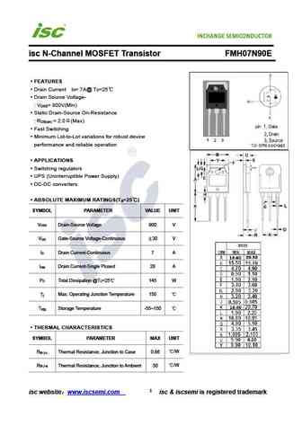
isc N-Channel MOSFET Transistor FMH07N90E FEATURES Drain Current I = 7A@ T =25 D C Drain Source Voltage- V = 900V(Min) DSS Static Drain-Source On-Resistance R = 2.0 (Max) DS(on) Fast Switching Minimum Lot-to-Lot variations for robust device performance and reliable operation APPLICATIONS Switching regulators UPS (Uninterruptible Power Supply) DC-DC co... See More ⇒
0.20. Size:234K inchange semiconductor
7n90a.pdf
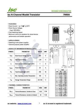
INCHANGE Semiconductor isc N-Channel Mosfet Transistor 7N90A FEATURES Drain Current I = 7A@ T =25 D C Drain Source Voltage- V = 900V(Min) DSS Fast Switching Speed Minimum Lot-to-Lot variations for robust device performance and reliable operation APPLICATIONS Switching mode power supplies General purpose power amplifier ABSOLUTE MAXIMUM RATINGS(T =25 ) a ... See More ⇒
Detailed specifications: 9N95, 9N100, 1N90, 2N90, 3N90, 4N90, 5N90, 6N90, IRF9540, 1N80, 2N80, 3N80, 4N80, 5N80, 6N80, 7N80, 8N80
Keywords - 7N90 MOSFET specs
7N90 cross reference
7N90 equivalent finder
7N90 pdf lookup
7N90 substitution
7N90 replacement
Learn how to find the right MOSFET substitute. A guide to cross-reference, check specs and replace MOSFETs in your circuits.