5N50 Datasheet. Specs and Replacement
Type Designator: 5N50 📄📄
Type of Transistor: MOSFET
Type of Control Channel: N-Channel
Absolute Maximum Ratings
Pd ⓘ - Maximum Power Dissipation: 125 W
|Vds|ⓘ - Maximum Drain-Source Voltage: 500 V
|Vgs|ⓘ - Maximum Gate-Source Voltage: 30 V
|Id| ⓘ - Maximum Drain Current: 5 A
Tj ⓘ - Maximum Junction Temperature: 150 °C
Electrical Characteristics
tr ⓘ - Rise Time: 46 nS
Cossⓘ - Output Capacitance: 80 pF
📄📄 Copy
5N50 substitution
- MOSFET ⓘ Cross-Reference Search
5N50 datasheet
5n50.pdf
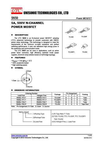
UNISONIC TECHNOLOGIES CO., LTD 5N50 Power MOSFET 5A, 500V N-CHANNEL POWER MOSFET 1 1 DESCRIPTION TO-220F TO-262 The UTC 5N50 is an N-channel power MOSFET adopting UTC s advanced technology to provide customers with DMOS, planar stripe technology. This technology is designed to meet the requirements of the minimum on-state resistance and perfect switching performance. It... See More ⇒
5n50.pdf
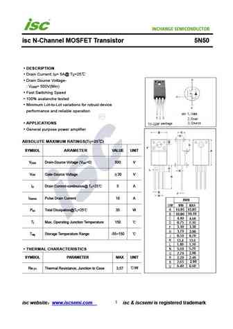
isc N-Channel MOSFET Transistor 5N50 DESCRIPTION Drain Current I = 5A@ T =25 D C Drain Source Voltage- V = 500V(Min) DSS Fast Switching Speed 100% avalanche tested Minimum Lot-to-Lot variations for robust device performance and reliable operation APPLICATIONS General purpose power amplifier ABSOLUTE MAXIMUM RATINGS(T =25 ) C SYMBOL ARAMETER VALUE UNIT V D... See More ⇒
cs25n50akr.pdf
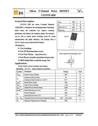
Silicon N-Channel Power MOSFET R CS25N50 AKR General Description VDSS 500 V CS25N50 AKR the silicon N-channel Enhanced ID 25 A PD(TC=25 ) 300 W VDMOSFET, is obtained by the self-aligned planar Technology RDS(ON)Typ 0.21 which reduce the conduction loss, improve switching performance and enhance the avalanche energy. The transistor can be used in various po... See More ⇒
ste24n90 ste36n50-da ste36n50-dk ste38n60 ste38na50 ste45n50 ste50n40 ste90n25.pdf
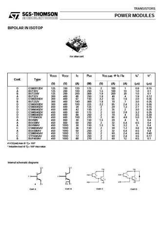
TRANSISTORS POWER MODULES BIPOLAR IN ISOTOP For other conf. VCEO VCEV IC Ptot VCE (sat) @IC / IB ts* tf* Conf. Type (V) (V) (A) (W) (V) (A) (A) ( s) ( s) D ESM2012DV 125 150 120 175 2 100 1 0.9 0.15 A BUT30V 125 200 100 250 1.5 100 10 1.0 0.1 B BUT230V 125 200 200 300 1.9 200 20 1.0 0.1 A BUT32V 300 400 80 250 1.9 40 4 1.9 0.12 D ESM2030DV 300 400 67 150 2.2 56 1.6 2.0 0.35 B BUT2... See More ⇒

mtv25n50e.pdf
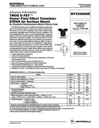
MOTOROLA Order this document SEMICONDUCTOR TECHNICAL DATA by MTV25N50E/D Advance Information MTV25N50E TMOS E-FET. Power Field Effect Transistor D3PAK for Surface Mount TMOS POWER FET N Channel Enhancement Mode Silicon Gate 25 AMPERES 500 VOLTS The D3PAK package has the capability of housing the largest chip RDS(on) = 0.200 OHM size of any standard, plastic, surface mount ... See More ⇒
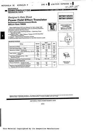
mtm15n45 mtm15n50.pdf
This Material Copyrighted By Its Respective Manufacturer This Material Copyrighted By Its Respective Manufacturer This Material Copyrighted By Its Respective Manufacturer This Material Copyrighted By Its Respective Manufacturer This Material Copyrighted By Its Respective Manufacturer ... See More ⇒
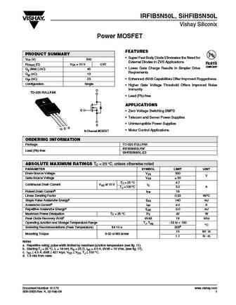
irfib5n50l.pdf
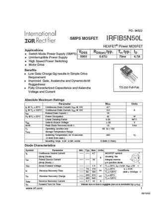
PD - 94522 SMPS MOSFET IRFIB5N50L HEXFET Power MOSFET Applications VDSS RDS(on) typ. Trr typ. ID l Switch Mode Power Supply (SMPS) 500V 0.67 73ns 4.7A l Uninterruptible Power Supply l High Speed Power Switching l Motor Drive Benefits l Low Gate Charge Qg results in Simple Drive Requirement l Improved Gate, Avalanche and Dynamicdv/dt Ruggedness TO-220 Full-Pak l Fully Chara... See More ⇒
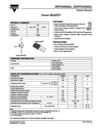
irfps35n50lpbf.pdf
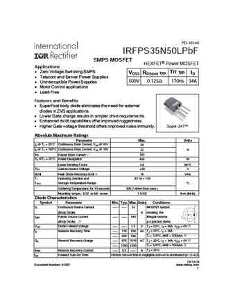
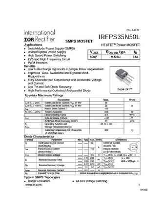
PD- 95140 IRFPS35N50LPbF SMPS MOSFET HEXFET Power MOSFET Applications Zero Voltage Switching SMPS Trr typ. VDSS RDS(on) typ. ID Telecom and Server Power Supplies 500V 0.125 170ns 34A Uninterruptible Power Supplies Motor Control applications Lead-Free Features and Benefits SuperFast body diode eliminates the need for external diodes in ZVS applications.... See More ⇒
irfps35n50l.pdf
PD- 94227 IRFPS35N50L SMPS MOSFET Applications HEXFET Power MOSFET l Switch Mode Power Supply (SMPS) l Uninterruptible Power Supply VDSS RDS(on) typ. ID l High Speed Power Switching 500V 0.125 34A l ZVS and High Frequency Circuit l PWM Inverters Benefits l Low Gate Charge Qg results in Simple Drive Requirement l Improved Gate, Avalanche and Dynamicdv/dt Ruggedness l Fully Ch... See More ⇒
irfib5n50lpbf.pdf
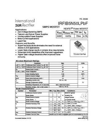
PD - 95390 IRFIB5N50LPbF SMPS MOSFET HEXFET Power MOSFET Applications Zero Voltage Switching SMPS Trr typ. VDSS RDS(on) typ. ID Telecom and Server Power Supplies 500V 0.67 73ns 4.7A Uninterruptible Power Supplies Motor Control applications Lead-Free Features and Benefits SuperFast body diode eliminates the need for external diodes in ZVS applications.... See More ⇒
phx5n50e 1.pdf
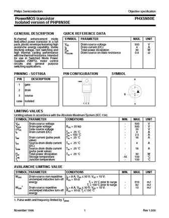
Philips Semiconductors Objective specification PowerMOS transistor PHX5N50E Isolated version of PHP8N50E GENERAL DESCRIPTION QUICK REFERENCE DATA N-channel enhancement mode SYMBOL PARAMETER MAX. UNIT field-effect power transistor in a full pack, plastic envelope featuring high VDS Drain-source voltage 500 V avalanche energy capability, stable ID Drain current (DC) 4 A blocking voltag... See More ⇒
std15n50m2ag.pdf
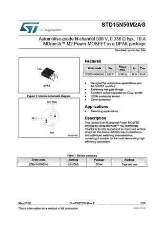
STD15N50M2AG Automotive-grade N-channel 500 V, 0.336 typ., 10 A MDmesh M2 Power MOSFET in a DPAK package Datasheet - production data Features R DS(on) Order code V I P DS D TOT max. STD15N50M2AG 500 V 0.380 10 A 85 W Designed for automotive applications and AEC-Q101 qualified Extremely low gate charge Excellent output capacitance (C ) profile OSS... See More ⇒
h5n5006ld h5n5006lm.pdf
To our customers, Old Company Name in Catalogs and Other Documents On April 1st, 2010, NEC Electronics Corporation merged with Renesas Technology Corporation, and Renesas Electronics Corporation took over all the business of both companies. Therefore, although the old company name remains in this document, it is a valid Renesas Electronics document. We appreciate your understanding. ... See More ⇒
rej03g1115 h5n5006ldlslmds.pdf

To our customers, Old Company Name in Catalogs and Other Documents On April 1st, 2010, NEC Electronics Corporation merged with Renesas Technology Corporation, and Renesas Electronics Corporation took over all the business of both companies. Therefore, although the old company name remains in this document, it is a valid Renesas Electronics document. We appreciate your understanding. ... See More ⇒
rej03g1116 h5n5007pds.pdf

To our customers, Old Company Name in Catalogs and Other Documents On April 1st, 2010, NEC Electronics Corporation merged with Renesas Technology Corporation, and Renesas Electronics Corporation took over all the business of both companies. Therefore, although the old company name remains in this document, it is a valid Renesas Electronics document. We appreciate your understanding. ... See More ⇒
rej03g0378 h5n5012p.pdf

To our customers, Old Company Name in Catalogs and Other Documents On April 1st, 2010, NEC Electronics Corporation merged with Renesas Technology Corporation, and Renesas Electronics Corporation took over all the business of both companies. Therefore, although the old company name remains in this document, it is a valid Renesas Electronics document. We appreciate your understanding. ... See More ⇒
rej03g1117 h5n5015pds.pdf

To our customers, Old Company Name in Catalogs and Other Documents On April 1st, 2010, NEC Electronics Corporation merged with Renesas Technology Corporation, and Renesas Electronics Corporation took over all the business of both companies. Therefore, although the old company name remains in this document, it is a valid Renesas Electronics document. We appreciate your understanding. ... See More ⇒
rej03g0175 h5n5016pl.pdf

To our customers, Old Company Name in Catalogs and Other Documents On April 1st, 2010, NEC Electronics Corporation merged with Renesas Technology Corporation, and Renesas Electronics Corporation took over all the business of both companies. Therefore, although the old company name remains in this document, it is a valid Renesas Electronics document. We appreciate your understanding. ... See More ⇒
rej03g0397 h5n5006dlds.pdf

To our customers, Old Company Name in Catalogs and Other Documents On April 1st, 2010, NEC Electronics Corporation merged with Renesas Technology Corporation, and Renesas Electronics Corporation took over all the business of both companies. Therefore, although the old company name remains in this document, it is a valid Renesas Electronics document. We appreciate your understanding. ... See More ⇒
h5n5004pl-e0-e.pdf
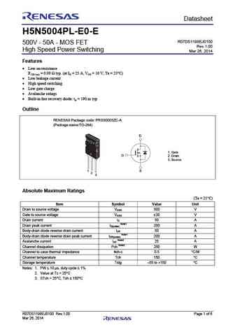
Preliminary Datasheet H5N5004PL-E0-E R07DS1198EJ0100 500V - 50A - MOS FET Rev.1.00 High Speed Power Switching Mar 26, 2014 Features Low on-resistance R DS (on) = 0.09 typ. (at ID = 25 A, VGS = 10 V, Ta = 25 C) Low leakage current High speed switching Low gate charge Avalanche ratings Built-in fast recovery diode trr = 190 ns typ Outline ... See More ⇒
rej03g1112 h5n5001fmds.pdf

To our customers, Old Company Name in Catalogs and Other Documents On April 1st, 2010, NEC Electronics Corporation merged with Renesas Technology Corporation, and Renesas Electronics Corporation took over all the business of both companies. Therefore, although the old company name remains in this document, it is a valid Renesas Electronics document. We appreciate your understanding. ... See More ⇒
h5n5005pl-e0-e.pdf
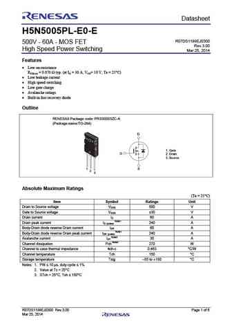
Preliminary Datasheet H5N5005PL-E0-E R07DS1199EJ0300 500V - 60A - MOS FET Rev.3.00 High Speed Power Switching Mar 25, 2014 Features Low on-resistance RDS(on) = 0.070 typ. (at ID = 30 A, VGS= 10 V, Ta = 25 C) Low leakage current High speed switching Low gate charge Avalanche ratings Built-in fast recovery diode Outline RENESAS Package cod... See More ⇒
rej03g1114 h5n5006fmds.pdf

To our customers, Old Company Name in Catalogs and Other Documents On April 1st, 2010, NEC Electronics Corporation merged with Renesas Technology Corporation, and Renesas Electronics Corporation took over all the business of both companies. Therefore, although the old company name remains in this document, it is a valid Renesas Electronics document. We appreciate your understanding. ... See More ⇒
rej03g1113 h5n5004plds.pdf

To our customers, Old Company Name in Catalogs and Other Documents On April 1st, 2010, NEC Electronics Corporation merged with Renesas Technology Corporation, and Renesas Electronics Corporation took over all the business of both companies. Therefore, although the old company name remains in this document, it is a valid Renesas Electronics document. We appreciate your understanding. ... See More ⇒
rej03g0419 h5n5005plds.pdf

To our customers, Old Company Name in Catalogs and Other Documents On April 1st, 2010, NEC Electronics Corporation merged with Renesas Technology Corporation, and Renesas Electronics Corporation took over all the business of both companies. Therefore, although the old company name remains in this document, it is a valid Renesas Electronics document. We appreciate your understanding. ... See More ⇒
h5n5016pl-e0-e.pdf
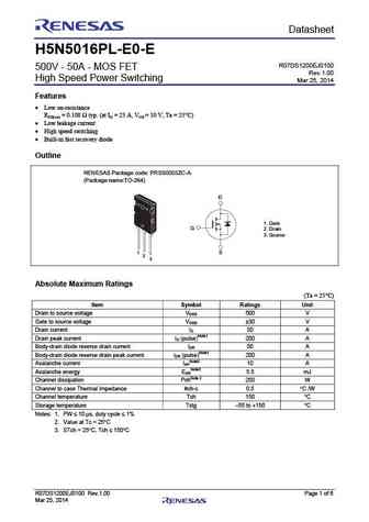
Preliminary Datasheet H5N5016PL-E0-E R07DS1200EJ0100 500V - 50A - MOS FET Rev.1.00 High Speed Power Switching Mar 25, 2014 Features Low on-resistance RDS(on) = 0.108 typ. (at ID = 25 A, VGS = 10 V, Ta = 25 C) Low leakage current High speed switching Built-in fast recovery diode Outline RENESAS Package code PRSS0003ZC-A (Package name TO-264) D 1.... See More ⇒
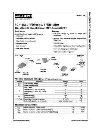
fdh15n50 fdp15n50 fdb15n50.pdf
August 2003 FDH15N50 / FDP15N50 / FDB15N50 15A, 500V, 0.38 Ohm, N-Channel SMPS Power MOSFET Applications Features Low Gate Charge Qg results in Simple Drive Switch Mode Power Supplies(SMPS), such as Requirement PFC Boost Improved Gate, Avalanche and High Reapplied dv/dt Two-Switch Forward Converter Ruggedness Single Switch Forward Converter Reduced rDS(ON) ... See More ⇒
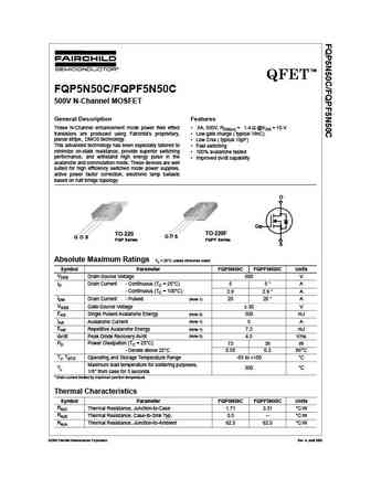
fqp5n50c fqp5n50c fqpf5n50c fqpf5n50c fqpf5n50ct fqpf5n50cttu fqpf5n50cydtu.pdf
... See More ⇒
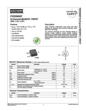
fdd5n50u.pdf

December 2007 TM Ultra FRFET FDD5N50U tm N-Channel MOSFET, FRFET 500V, 3A, 2.0 Features Description RDS(on) = 1.65 ( Typ.)@ VGS = 10V, ID = 1.5A These N-Channel enhancement mode power field effect transis- tors are produced using Fairchild s proprietary, planar stripe, Low gate charge ( Typ. 11nC) DOMS technology. Low Crss ( Typ. 5pF) This advance technology h... See More ⇒
fqb5n50ctm fqb5n50c fqi5n50c fqi5n50ctu.pdf
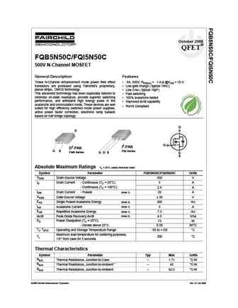
October 2008 QFET FQB5N50C/FQI5N50C 500V N-Channel MOSFET General Description Features These N-Channel enhancement mode power field effect 5A, 500V, RDS(on) = 1.4 @VGS = 10 V transistors are produced using Fairchild s proprietary, Low gate charge ( typical 18nC) planar stripe, DMOS technology. Low Crss ( typical 15pF) This advanced technology has been especially tai... See More ⇒
fdp5n50 fdpf5n50.pdf
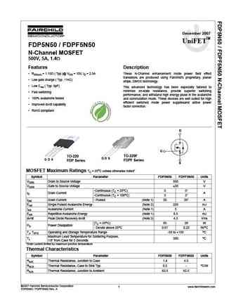
December 2007 UniFETTM FDP5N50 / FDPF5N50 tm N-Channel MOSFET 500V, 5A, 1.4 Features Description RDS(on) = 1.15 ( Typ.)@ VGS = 10V, ID = 2.5A These N-Channel enhancement mode power field effect transistors are produced using Fairchild s proprietary, planar Low gate charge ( Typ. 11nC) stripe, DMOS technology. Low Crss ( Typ. 5pF) This advanced technology has bee... See More ⇒
fdh15n50 fdp15n50.pdf

August 2003 FDH15N50 / FDP15N50 / FDB15N50 15A, 500V, 0.38 Ohm, N-Channel SMPS Power MOSFET Applications Features Low Gate Charge Qg results in Simple Drive Switch Mode Power Supplies(SMPS), such as Requirement PFC Boost Improved Gate, Avalanche and High Reapplied dv/dt Two-Switch Forward Converter Ruggedness Single Switch Forward Converter Reduced rDS(ON) ... See More ⇒
fdp5n50.pdf
May 2012 UniFETTM FDP5N50 / FDPF5N50T tm N-Channel MOSFET 500V, 5A, 1.4 Features Description RDS(on) = 1.15 ( Typ.)@ VGS = 10V, ID = 2.5A These N-Channel enhancement mode power field effect transistors are produced using Fairchild s proprietary, planar Low gate charge ( Typ. 11nC) stripe, DMOS technology. Low Crss ( Typ. 5pF) This advanced technology has been es... See More ⇒
fqd5n50.pdf
TIGER ELECTRONIC CO.,LTD 500V N-Channel MOSFET FQD5N50 DESCRIPTION These N-Channel enhancement mode power field effect transistors are produced using Fairchild s proprietary, planar stripe, DMOS technology. This advanced technology has been especially tailored to minimize on-state resistance, provide superior switching performance, and withstand high energy pulse in the avalanche an... See More ⇒
fqb5n50cf fqb5n50cftm.pdf
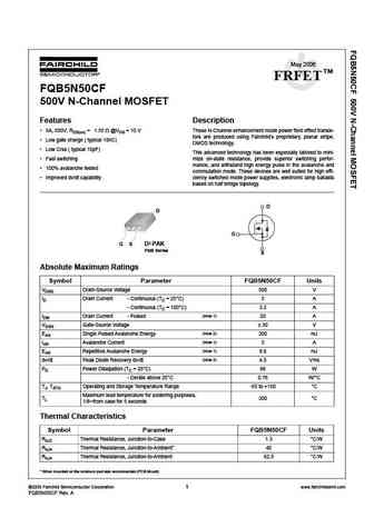
May 2006 TM FRFET FQB5N50CF 500V N-Channel MOSFET Features Description 5A, 500V, RDS(on) = 1.55 @VGS = 10 V These N-Channel enhancement mode power field effect transis- tors are produced using Fairchild s proprietary, planar stripe, Low gate charge ( typical 18nC) DMOS technology. Low Crss ( typical 15pF) This advanced technology has been especially tailored to mini... See More ⇒
fdd5n50f.pdf
December 2007 UniFETTM FDD5N50F tm N-Channel MOSFET, FRFET 500V, 3.5A, 1.55 Features Description RDS(on) = 1.25 ( Typ.)@ VGS = 10V, ID = 1.75A These N-Channel enhancement mode power field effect transistors are produced using Fairchild s proprietary, planar Low gate charge ( Typ. 11nC) stripe, DMOS technology. Low Crss ( Typ. 5pF) This advanced technology has ... See More ⇒
fdd5n50.pdf
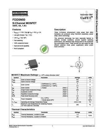
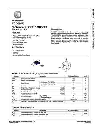
December 2007 UniFETTM FDD5N50 tm N-Channel MOSFET 500V, 4A, 1.4 Features Description RDS(on) = 1.15 ( Typ.)@ VGS = 10V, ID = 2A These N-Channel enhancement mode power field effect transistors are produced using Fairchild s proprietary, planar Low gate charge ( Typ. 11nC) stripe, DMOS technology. Low Crss ( Typ. 5pF) This advanced technology has been especiall... See More ⇒
fdh45n50f.pdf
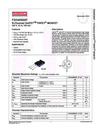
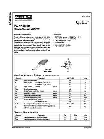
November 2013 FDH45N50F N-Channel UniFETTM FRFET MOSFET 500 V, 45 A, 120 m Features Description UniFETTM MOSFET is Fairchild Semiconductor s high voltage RDS(on) = 105 m (Typ.) @ VGS = 10 V, ID = 22.5 A MOSFET family based on planar stripe and DMOS technology. Low Gate Charge (Typ. 105 nC) This MOSFET is tailored to reduce on-state resistance, and to provide better swi... See More ⇒
fdp5n50nz fdpf5n50nz.pdf
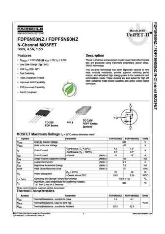
March 2010 UniFET-IITM FDP5N50NZ / FDPF5N50NZ tm N-Channel MOSFET 500V, 4.5A, 1.5 Features Description RDS(on) = 1.38 (Typ.)@ VGS = 10V, ID = 2.25A These N-Channel enhancement mode power field effect transis tors are produced using Fairchild s proprietary, planar stripe, Low Gate Charge (Typ. 9nC) DMOS technology. Low Crss (Typ. 4pF) This advance technology has b... See More ⇒
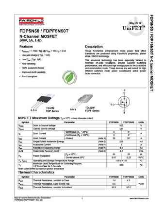
fdpf5n50t.pdf
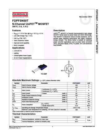
November 2013 FDPF5N50T N-Channel UniFETTM MOSFET 500 V, 5 A, 1.4 Features Description RDS(on) = 1.15 (Typ.) @ VGS = 10 V, ID = 2.5 A UniFETTM MOSFET is Fairchild Semiconductor s high voltage MOSFET family based on planar stripe and DMOS technology. Low Gate Charge (Typ. 11 nC) This MOSFET is tailored to reduce on-state resistance, and to Low Crss (Typ. 5 pF) provi... See More ⇒
fqd5n50c fqd5n50ctf fqd5n50ctm fqd5n50c fqu5n50c fqu5n50ctu.pdf
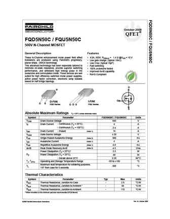
October 2008 QFET FQD5N50C / FQU5N50C 500V N-Channel MOSFET General Description Features These N-Channel enhancement mode power field effect 4.0A, 500V, RDS(on) = 1.4 @VGS = 10 V transistors are produced using Fairchild s proprietary, Low gate charge ( typical 18nC) planar stripe, DMOS technology. Low Crss ( typical 15pF) This advanced technology has been especially... See More ⇒
fdp5n50nzf fdpf5n50nzf.pdf
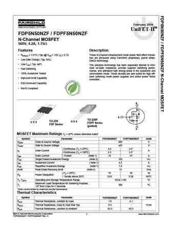
February 2010 TM UniFET-II FDP5N50NZF / FDPF5N50NZF tm N-Channel MOSFET 500V, 4.2A, 1.75 Features Description RDS(on) = 1.57 ( Typ.)@ VGS = 10V, ID = 2.1A These N-Channel enhancement mode power field effect transis- tors are produced using Fairchild s proprietary, planar stripe, Low Gate Charge ( Typ. 9nC) DMOS technology. Low Crss ( Typ. 4pF) This advanc... See More ⇒
fdp5n50f fdpf5n50ft.pdf
December 2007 UniFETTM FDP5N50F / FDPF5N50FT tm N-Channel MOSFET, FRFET 500V, 4.5A, 1.55 Features Description RDS(on) = 1.25 ( Typ.)@ VGS = 10V, ID = 2.25A These N-Channel enhancement mode power field effect transistors are produced using Fairchild s proprietary, planar Low gate charge ( Typ. 11nC) stripe, DMOS technology. Low Crss ( Typ. 5pF) This advanced tech... See More ⇒
fqd5n50tf fqu5n50tu.pdf
April 2000 TM QFET QFET QFET QFET 500V N-ChanneI MOSFET GeneraI Description Features These N-Channel enhancement mode power field effect 3.5A, 500V, RDS(on) = 1.8 @VGS = 10 V transistors are produced using Fairchild s proprietary, Low gate charge ( typical 13 nC) planar stripe, DMOS technology. Low Crss ( typical 8.5 pF) This advanced technology... See More ⇒
fdd5n50nz.pdf

November 2009 UniFET-IITM FDD5N50NZ N-Channel MOSFET 500V, 4A, 1.5 Features Description RDS(on) = 1.38 ( Typ.)@ VGS = 10V, ID = 2A These N-Channel enhancement mode power field effect transistors are produced using Fairchild s proprietary, planar Low Gate Charge ( Typ. 9nC) stripe, DMOS technology. Low Crss ( Typ. 4pF) This advance technology has been especially... See More ⇒
fdd5n50nzf.pdf
November 2009 UniFET-IITM FDD5N50NZF N-Channel MOSFET 500V, 3.7A, 1.75 Features Description RDS(on) = 1.47 ( Typ.)@ VGS = 10V, ID = 1.85A These N-Channel enhancement mode power field effect transistors are produced using Fairchild s proprietary, planar Low Gate Charge ( Typ. 9nC) stripe, DMOS technology. Low Crss ( Typ. 4pF) This advance technology has been esp... See More ⇒
fqpf5n50cf fqpf5n50cftu.pdf
TM FRFET FQPF5N50CF 500V N-Channel MOSFET Features Description 5A, 500V, RDS(on) = 1.55 @VGS = 10 V These N-Channel enhancement mode power field effect transis- tors are produced using Fairchild s proprietary, planar stripe, Low gate charge ( typical 18nC) DMOS technology. Low Crss ( typical 15pF) This advanced technology has been especially tailored to mini- F... See More ⇒
fdp5n50u fdpf5n50ut.pdf
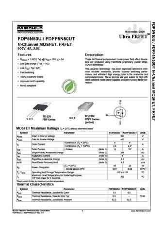
November2009 TM Ultra FRFET FDP5N50U / FDPF5N50UT tm N-Channel MOSFET, FRFET 500V, 4A, 2.0 Features Description RDS(on) = 1.65 ( Typ.)@ VGS = 10V, ID = 2A These N-Channel enhancement mode power field effect transis- tors are produced using Fairchild s proprietary, planar stripe, Low gate charge ( Typ. 11nC) DOMS technology. Low Crss ( Typ. 5pF) This advance tech... See More ⇒
fdp5n50nzu fdpf5n50nzu.pdf
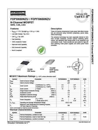
February 2010 TM UniFET-II FDP5N50NZU / FDPF5N50NZU tm N-Channel MOSFET 500V, 3.9A, 2.0 Features Description RDS(on) = 1.7 ( Typ.)@ VGS = 10V, ID = 1.95A These N-Channel enhancement mode power field effect transis- tors are produced using Fairchild s proprietary, planar stripe, Low Gate Charge ( Typ. 9nC) DMOS technology. Low Crss ( Typ. 4pF) This advance... See More ⇒
fqpf5n50.pdf
April 2000 TM QFET QFET QFET QFET 500V N-ChanneI MOSFET GeneraI Description Features These N-Channel enhancement mode power field effect 3.0A, 500V, RDS(on) = 1.8 @VGS = 10 V transistors are produced using Fairchild s proprietary, Low gate charge ( typical 13 nC) planar stripe, DMOS technology. Low Crss ( typical 8.5 pF) This advanced technology has been... See More ⇒
fqb5n50tm.pdf
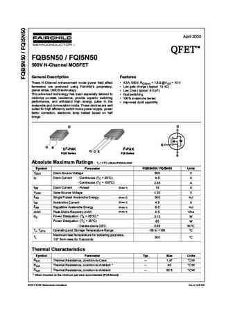
April 2000 TM QFET QFET QFET QFET 500V N-ChanneI MOSFET GeneraI Description Features These N-Channel enhancement mode power field effect 4.5A, 500V, RDS(on) = 1.8 @VGS = 10 V transistors are produced using Fairchild s proprietary, Low gate charge ( typical 13 nC) planar stripe, DMOS technology. Low Crss ( typical 8.5 pF) This advanced technology... See More ⇒
sihu5n50d.pdf
SiHU5N50D www.vishay.com Vishay Siliconix D Series Power MOSFET FEATURES PRODUCT SUMMARY Optimal Design VDS (V) at TJ max. 550 - Low Area Specific On-Resistance RDS(on) max. at 25 C ( ) VGS = 10 V 1.5 - Low Input Capacitance (Ciss) Qg (max.) (nC) 20 - Reduced Capacitive Switching Losses Qgs (nC) 3 - High Body Diode Ruggedness Qgd (nC) 5 - Avalanche Energy Rated (UIS) ... See More ⇒
sihp15n50e.pdf
SiHP15N50E www.vishay.com Vishay Siliconix E Series Power MOSFET FEATURES PRODUCT SUMMARY Low figure-of-merit (FOM) Ron x Qg VDS (V) at TJ max. 550 Low input capacitance (Ciss) RDS(on) max. at 25 C ( ) VGS = 10 V 0.243 Reduced switching and conduction losses Qg max. (nC) 66 Low gate charge (Qg) Qgs (nC) 8 Avalanche energy rated (UIS) Qgd (nC) 14 Materi... See More ⇒
sihd5n50d.pdf
SiHD5N50D www.vishay.com Vishay Siliconix D Series Power MOSFET FEATURES PRODUCT SUMMARY Optimal Design VDS (V) at TJ max. 550 - Low Area Specific On-Resistance RDS(on) max. at 25 C ( ) VGS = 10 V 1.5 - Low Input Capacitance (Ciss) Qg (max.) (nC) 20 - Reduced Capacitive Switching Losses - High Body Diode Ruggedness Qgs (nC) 3 Available - Avalanche Energy Rated (UIS) Qgd ... See More ⇒
sihf5n50d.pdf
SiHF5N50D www.vishay.com Vishay Siliconix D Series Power MOSFET FEATURES PRODUCT SUMMARY Optimal Design VDS (V) at TJ max. 550 - Low Area Specific On-Resistance RDS(on) max. at 25 C ( ) VGS = 10 V 1.5 - Low Input Capacitance (Ciss) Qg (max.) (nC) 20 - Reduced Capacitive Switching Losses Qgs (nC) 3 - High Body Diode Ruggedness Qgd (nC) 5 - Avalanche Energy Rated (UIS) Co... See More ⇒
irfps35n50lpbf.pdf
IRFPS35N50L, SiHFPS35N50L Vishay Siliconix Power MOSFET FEATURES PRODUCT SUMMARY Super Fast Body Diode Eliminates the Need for VDS (V) 500 Available External Diodes in ZVS Applications RDS(on) ( )VGS = 10 V 0.125 RoHS* Lower Gate Charge Results in Simpler Drive Qg (Max.) (nC) 230 COMPLIANT Requirements Qgs (nC) 65 Enhanced dV/dt Capabilities Offer Improved Ruggedne... See More ⇒
sihp25n50e.pdf

SiHP25N50E www.vishay.com Vishay Siliconix E Series Power MOSFET FEATURES PRODUCT SUMMARY Low figure-of-merit (FOM) Ron x Qg VDS (V) at TJ max. 550 Low input capacitance (Ciss) RDS(on) max. at 25 C ( ) VGS = 10 V 0.145 Reduced switching and conduction losses Qg (Max.) (nC) 86 Low gate charge (Qg) Qgs (nC) 14 Qgd (nC) 25 Avalanche energy rated (UIS) Config... See More ⇒
siha25n50e.pdf
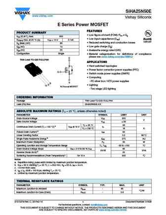
SiHA25N50E www.vishay.com Vishay Siliconix E Series Power MOSFET FEATURES PRODUCT SUMMARY Low figure-of-merit (FOM) Ron x Qg VDS (V) at TJ max. 550 Low input capacitance (Ciss) RDS(on) max. at 25 C ( ) VGS = 10 V 0.145 Reduced switching and conduction losses Qg (Max.) (nC) 86 Low gate charge (Qg) Qgs (nC) 14 Qgd (nC) 25 Avalanche energy rated (UIS) Config... See More ⇒
siha15n50e.pdf
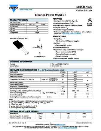
SiHA15N50E www.vishay.com Vishay Siliconix E Series Power MOSFET FEATURES PRODUCT SUMMARY Low figure-of-merit (FOM) Ron x Qg VDS (V) at TJ max. 550 Low input capacitance (Ciss) RDS(on) max. at 25 C ( ) VGS = 10 V 0.243 Reduced switching and conduction losses Qg max. (nC) 66 Low gate charge (Qg) Qgs (nC) 8 Avalanche energy rated (UIS) Qgd (nC) 14 Materi... See More ⇒
sihb15n50e.pdf
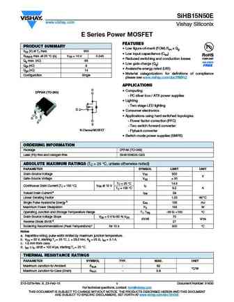
SiHB15N50E www.vishay.com Vishay Siliconix E Series Power MOSFET FEATURES PRODUCT SUMMARY Low figure-of-merit (FOM) Ron x Qg VDS (V) at TJ max. 550 Low input capacitance (Ciss) RDS(on) max. at 25 C ( ) VGS = 10 V 0.243 Reduced switching and conduction losses Qg max. (nC) 66 Low gate charge (Qg) Qgs (nC) 8 Avalanche energy rated (UIS) Qgd (nC) 14 Materi... See More ⇒
irfib5n50lpbf.pdf
IRFIB5N50L, SiHFIB5N50L Vishay Siliconix Power MOSFET FEATURES PRODUCT SUMMARY Super Fast Body Diode Eliminates the Need for VDS (V) 500 External Diodes in ZVS Applications RoHS RDS(on) ( )VGS = 10 V 0.67 COMPLIANT Lower Gate Charge Results in Simpler Drive Qg (Max.) (nC) 45 Reqirements Qgs (nC) 13 Qgd (nC) 23 Enhanced dV/dt Capabilities Offer Improved Ruggedness ... See More ⇒
sihp5n50d.pdf
SiHP5N50D www.vishay.com Vishay Siliconix D Series Power MOSFET FEATURES PRODUCT SUMMARY Optimal Design VDS (V) at TJ max. 550 - Low Area Specific On-Resistance RDS(on) max. at 25 C ( ) VGS = 10 V 1.5 - Low Input Capacitance (Ciss) Qg (max.) (nC) 20 - Reduced Capacitive Switching Losses Qgs (nC) 3 - High Body Diode Ruggedness Qgd (nC) 5 - Avalanche Energy Rated (UIS) ... See More ⇒
sihg25n50e.pdf
SiHG25N50E www.vishay.com Vishay Siliconix E Series Power MOSFET FEATURES PRODUCT SUMMARY Low figure-of-merit (FOM) Ron x Qg VDS (V) at TJ max. 550 Low input capacitance (Ciss) RDS(on) max. at 25 C ( ) VGS = 10 V 0.145 Reduced switching and conduction losses Qg (Max.) (nC) 86 Low gate charge (Qg) Qgs (nC) 14 Qgd (nC) 25 Avalanche energy rated (UIS) Config... See More ⇒
ixfk33n50 ixfk35n50.pdf
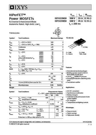
VDSS ID25 RDS(on) HiPerFETTM IXFK33N50 500 V 33 A 0.16 W Power MOSFETs IXFK35N50 500 V 35 A 0.15 W N-Channel Enhancement Mode trr 250 ns Avalanche Rated, High dv/dt, Low trr Preliminary data TO-264 AA Symbol Test Conditions Maximum Ratings VDSS TJ = 25 C to 150 C 500 V VDGR TJ = 25 C to 150 C; RGS = 1 MW 500 V G VGS Continuous 20 V D (TAB) D S VGSM Transient 30 V ID... See More ⇒
ixfx50n50 ixfx55n50.pdf
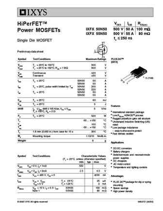
VDSS ID25 RDS(on) HiPerFETTM IXFX 50N50 500 V 50 A 100 m Power MOSFETs IXFX 55N50 500 V 55 A 80 m trr 250 ns Single Die MOSFET Preliminary data sheet Symbol Test Conditions Maximum Ratings PLUS 247TM (IXFX) VDSS TJ = 25 C to 150 C 500 V VDGR TJ = 25 C to 150 C; RGS = 1 M 500 V VGS Continuous 20 V VGSM ... See More ⇒
ixfk55n50 ixfx55n50 ixfn55n50.pdf
VDSS = 500 V IXFK 55N50 HiPerFETTM ID25 = 55 A IXFX 55N50 Power MOSFET RDS(on) = 90m IXFN 55N50 250 ns trr Single Die MOSFET Symbol Test Conditions Maximum Ratings PLUS247(IXFX) VDSS TJ = 25 C to 150 C 500 V VDGR TJ = 25 C to 150 C 500 V VGSS Continuous 20 V VGSM Transient 30 V (TAB) G C ID25 TC = 25 C55 A E IDM TC = 2... See More ⇒
ixfk50n50 ixfn50n50 ixfk55n50 ixfn55n50.pdf
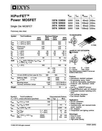
VDSS ID25 RDS(on) trr HiPerFETTM Power MOSFET IXFN 55N50 500V 55A 80m 250ns IXFN 50N50 500V 50A 100m 250ns IXFK 55N50 500V 55A 80m 250ns Single Die MOSFET IXFK 50N50 500V 50A 100m 250ns Preliminary data sheet TO-264 AA (IXFK) Symbol Test Conditions Maximum Ratings IXFN IXFK IXFK IXFN 55N50 50N50 55N50 50N50 VDSS TJ = 25 C to 150 C 500 500 V VDGR TJ = 25 C to 150 C... See More ⇒
ixfa5n50p3 ixfp5n50p3 ixfy5n50p3.pdf
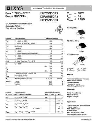
Advance Technical Information Polar3 TM HiPerFETTM VDSS = 500V IXFY5N50P3 Power MOSFETs ID25 = 5A IXFA5N50P3 RDS(on) 1.65 IXFP5N50P3 N-Channel Enhancement Mode Avalanche Rated TO-252 (IXFY) Fast Intrinsic Rectifier G S D (Tab) Symbol Test Conditions Maximum Ratings VDSS TJ = 25 C to 150 C 500 V TO-263 AA (IXFA) VDGR TJ = 25 C to 150 C, R... See More ⇒
ixfn55n50f.pdf
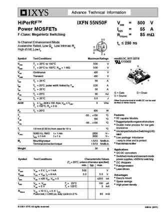
Advance Technical Information HiPerRFTM IXFN 55N50F VDSS = 500 V Power MOSFETs ID25 = 55 A F-Class MegaHertz Switching RDS(on) = 85 m D N-Channel Enhancement Mode trr 250 ns Avalanche Rated, Low Qg, Low Intrinsic R G g High dV/dt, Low t rr S S Symbol Test Conditions Maximum Ratings miniBLOC, SOT-227 B E153432 VDSS TJ = 25 C to ... See More ⇒
ixfr50n50 ixfr55n50.pdf
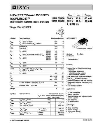
VDSS ID25 RDS(on) HiPerFETTM Power MOSFETs IXFR 50N50 500 V 43 A 100 m ISOPLUS247TM IXFR 55N50 500 V 48 A 90 m (Electrically Isolated Back Surface) trr 250 ns Single Die MOSFET Symbol Test Conditions Maximum Ratings ISOPLUS 247TM VDSS TJ = 25 C to 150 C 500 V VDGR TJ = 25 C to 150 C; RGS = 1 M 500 V G VGS... See More ⇒
ixta15n50l2.pdf
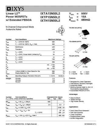
Linear L2TM VDSS = 500V IXTA15N50L2 Power MOSFETs ID25 = 15A IXTP15N50L2 RDS(on) 480m w/ Extended FBSOA IXTH15N50L2 N-Channel Enhancement Mode TO-263 AA (IXTA) Avalanche Rated G S D (Tab) Symbol Test Conditions Maximum Ratings TO-220AB (IXTP) VDSS TJ = 25 C to 150 C 500 V VDGR TJ = 25 C to 150 C, RGS = 1M 500 V VGSS Continuous 20 V ... See More ⇒
ixth15n50l2-ixtp15n50l2.pdf
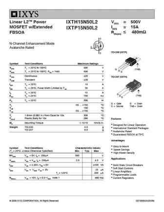
Linear L2TM Power VDSS = 500V IXTH15N50L2 MOSFET w/Extended ID25 = 15A IXTP15N50L2 RDS(on) 480m FBSOA N-Channel Enhancement Mode Avalanche Rated TO-220 (IXTP) Symbol Test Conditions Maximum Ratings VDSS TJ = 25 C to 150 C 500 V G (TAB) D VDGR TJ = 25 C to 150 C, RGS = 1M 500 V S VGSS Continuous 20 V TO-247 (IXTH) VGSM Transient 30... See More ⇒
fdu5n50nztu.pdf
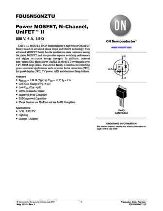
FDU5N50NZTU Power MOSFET, N-Channel, UniFETt II 500 V, 4 A, 1.5 W UniFET II MOSFET is ON Semiconductor s high voltage MOSFET www.onsemi.com family based on advanced planar stripe and DMOS technology. This advanced MOSFET family has the smallest on-state resistance among the planar MOSFET, and also provides superior switching performance D and higher avalanche energy strength. In add... See More ⇒
ndf05n50z ndp05n50z ndd05n50z.pdf
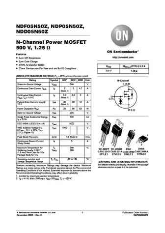
NDF05N50Z, NDP05N50Z, NDD05N50Z N-Channel Power MOSFET 500 V, 1.25 W Features http //onsemi.com Low ON Resistance Low Gate Charge 100% Avalanche Tested VDSS RDS(on) (TYP) @ 2.2 A These Devices are Pb-Free and are RoHS Compliant 500 V 1.25 W ABSOLUTE MAXIMUM RATINGS (TC = 25 C unless otherwise noted) Rating Symbol NDF NDP NDD Unit N-Channel D (2) Drain-to-Source... See More ⇒
fqp5n50c fqpf5n50c.pdf

Is Now Part of To learn more about ON Semiconductor, please visit our website at www.onsemi.com ON Semiconductor and the ON Semiconductor logo are trademarks of Semiconductor Components Industries, LLC dba ON Semiconductor or its subsidiaries in the United States and/or other countries. ON Semiconductor owns the rights to a number of patents, trademarks, copyrights, trade secrets, and oth... See More ⇒
fdd5n50u.pdf
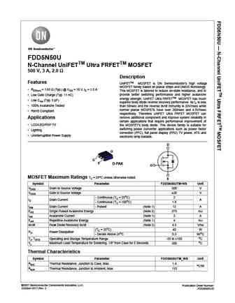
FDD5N50U N-Channel UniFETTM Ultra FRFETTM MOSFET 500 V, 3 A, 2.0 Description Features UniFETTM MOSFET is ON Semiconductor s high voltage MOSFET family based on planar stripe and DMOS technology. RDS(on) = 1.65 (Typ.) @ VGS = 10 V, ID = 1.5 A This MOSFET is tailored to reduce on-state resistance, and to Low Gate Charge (Typ. 11 nC) provide better switching performance... See More ⇒
fdpf5n50nzu.pdf

Is Now Part of To learn more about ON Semiconductor, please visit our website at www.onsemi.com Please note As part of the Fairchild Semiconductor integration, some of the Fairchild orderable part numbers will need to change in order to meet ON Semiconductor s system requirements. Since the ON Semiconductor product management systems do not have the ability to manage part nomenclatur... See More ⇒
fdd5n50.pdf
FDD5N50 N-Channel UniFETTM MOSFET Description 500 V, 4 A, 1.4 UniFETTM MOSFET is ON Semiconductor s high voltage Features MOSFET family based on planar stripe and DMOS technology. This MOSFET is tailored to reduce on-state resistance, and to RDS(on) = 1.15 (Typ.) @ VGS = 10 V, ID = 2 A provide better switching performance and higher avalanche Low Gate Charge (Typ. ... See More ⇒
fdpf5n50t.pdf

Is Now Part of To learn more about ON Semiconductor, please visit our website at www.onsemi.com Please note As part of the Fairchild Semiconductor integration, some of the Fairchild orderable part numbers will need to change in order to meet ON Semiconductor s system requirements. Since the ON Semiconductor product management systems do not have the ability to manage part nomenclatur... See More ⇒
fdb15n50.pdf

Is Now Part of To learn more about ON Semiconductor, please visit our website at www.onsemi.com Please note As part of the Fairchild Semiconductor integration, some of the Fairchild orderable part numbers will need to change in order to meet ON Semiconductor s system requirements. Since the ON Semiconductor product management systems do not have the ability to manage part nomenclatur... See More ⇒
fdd5n50ftm-ws.pdf
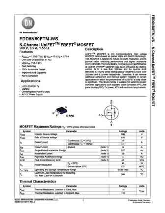
FDD5N50FTM-WS N-Channel UniFETTM FRFET MOSFET 500 V, 3.5 A, 1.55 Description Features UniFETTM MOSFET is ON Semiconductor s high voltage RDS(on) = 1.25 (Typ.) @ VGS = 10 V, ID = 1.75 A MOSFET family based on planar stripe and DMOS technology. This MOSFET is tailored to reduce on-state resistance, and to Low Gate Charge (Typ. 11 nC) provide better switching performa... See More ⇒
fdd5n50nz.pdf

Is Now Part of To learn more about ON Semiconductor, please visit our website at www.onsemi.com Please note As part of the Fairchild Semiconductor integration, some of the Fairchild orderable part numbers will need to change in order to meet ON Semiconductor s system requirements. Since the ON Semiconductor product management systems do not have the ability to manage part nomenclatur... See More ⇒

5n50l-tf3-t 5n50g-tf3-t 5n50l-tf1-t 5n50g-tf1-t 5n50l-tn3-r 5n50g-tn3-r 5n50l-t2q-t 5n50g-t2q-t.pdf
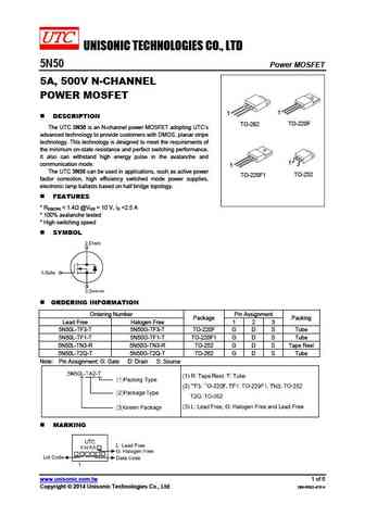
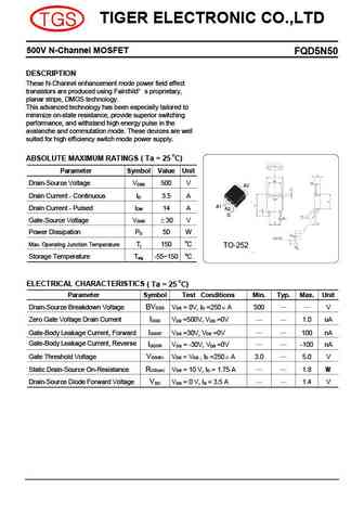
UNISONIC TECHNOLOGIES CO., LTD 5N50 Power MOSFET 5A, 500V N-CHANNEL POWER MOSFET 1 1 DESCRIPTION TO-220F TO-262 The UTC 5N50 is an N-channel power MOSFET adopting UTC s advanced technology to provide customers with DMOS, planar stripe technology. This technology is designed to meet the requirements of the minimum on-state resistance and perfect switching performance. ... See More ⇒
15n50.pdf
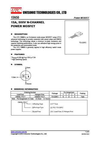
UNISONIC TECHNOLOGIES CO., LTD 15N50 Power MOSFET 15A, 500V N-CHANNEL POWER MOSFET DESCRIPTION The UTC 15N50 is an N-channel mode power MOSFET using UTC s 1 advanced technology to provide customers with planar stripe and DMOS technology. This technology allows a minimum on-state resistance and TO-220F2 superior switching performance. It also can withstand high energy puls... See More ⇒
5n50k.pdf
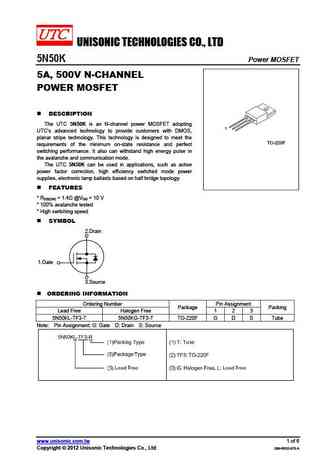
UNISONIC TECHNOLOGIES CO., LTD 5N50K Power MOSFET 5A, 500V N-CHANNEL POWER MOSFET DESCRIPTION The UTC 5N50K is an N-channel power MOSFET adopting 1 UTC s advanced technology to provide customers with DMOS, planar stripe technology. This technology is designed to meet the TO-220F requirements of the minimum on-state resistance and perfect switching performance. It also can... See More ⇒
fmi05n50e.pdf
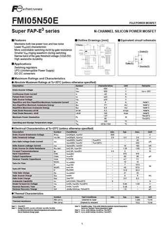
FMI05N50E FUJI POWER MOSFET Super FAP-E3 series N-CHANNEL SILICON POWER MOSFET Features Outline Drawings [mm] Equivalent circuit schematic Maintains both low power loss and low noise T-Pack(L) Lower R (on) characteristic DS More controllable switching dv/dt by gate resistance Drain(D) Smaller V ringing waveform during switching GS Narrow band of the gate threshold voltage (3.0 0.5V)... See More ⇒
fmc05n50e.pdf
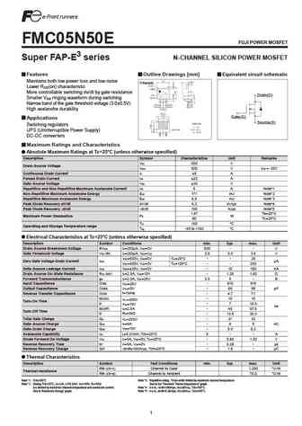
FMC05N50E FUJI POWER MOSFET Super FAP-E3 series N-CHANNEL SILICON POWER MOSFET Features Outline Drawings [mm] Equivalent circuit schematic Maintains both low power loss and low noise T-Pack(S) Lower R (on) characteristic DS More controllable switching dv/dt by gate resistance Drain(D) Smaller V ringing waveform during switching GS Narrow band of the gate threshold voltage (3.0 0.5V)... See More ⇒
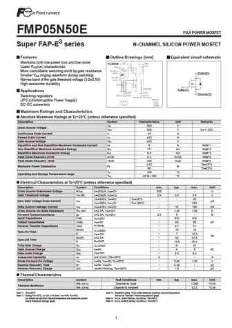
fmv05n50e.pdf
FMV05N50E FUJI POWER MOSFET Super FAP-E3 series N-CHANNEL SILICON POWER MOSFET Features Outline Drawings [mm] Equivalent circuit schematic Maintains both low power loss and low noise TO-220F(SLS) Lower R (on) characteristic DS More controllable switching dv/dt by gate resistance Drain(D) Smaller V ringing waveform during switching GS Narrow band of the gate threshold voltage (3.0 0.... See More ⇒
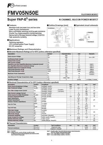
fmp05n50e.pdf
FMP05N50E FUJI POWER MOSFET Super FAP-E3 series N-CHANNEL SILICON POWER MOSFET Features Outline Drawings [mm] Equivalent circuit schematic Maintains both low power loss and low noise TO-220AB Lower R (on) characteristic DS More controllable switching dv/dt by gate resistance Drain(D) Smaller V ringing waveform during switching GS Narrow band of the gate threshold voltage (3.0 0.5V) ... See More ⇒
ssq5n50.pdf
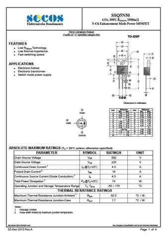
SSQ5N50 4.5A, 500V, RDS(ON) 1500m N-Ch Enhancement Mode Power MOSFET Elektronische Bauelemente RoHS Compliant Product A suffix of -C specifies halogen free TO-220P D FEATURES C Low RDS(on) Technology. B Low thermal impedance. R T Fast switching speed. A E S G APPLICATIONS F I Electronic ballast. H Electronic transformer J K ... See More ⇒
tsm15n50ci.pdf
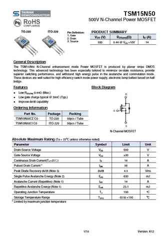
TSM15N50 500V N-Channel Power MOSFET TO-220 ITO-220 PRODUCT SUMMARY Pin Definition 1. Gate VDS (V) RDS(on)( ) ID (A) 2. Drain 3. Source 500 0.44 @ VGS =10V 14 General Description The TSM15N50 N-Channel enhancement mode Power MOSFET is produced by planar stripe DMOS technology. This advanced technology has been especially tailored to minimize on-state resistance, pro... See More ⇒
kf5n50f.pdf
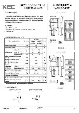
KF5N50P/F/PZ/FZ SEMICONDUCTOR N CHANNEL MOS FIELD TECHNICAL DATA EFFECT TRANSISTOR General Description KF5N50P, KF5N50PZ A This planar stripe MOSFET has better characteristics, such as fast O C switching time, low on resistance, low gate charge and excellent F avalanche characteristics. It is mainly suitable for electronic ballast and E DIM MILLIMETERS G _ + switching mode pow... See More ⇒
kf5n50pz.pdf
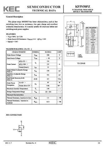
KF5N50PZ SEMICONDUCTOR N CHANNEL MOS FIELD TECHNICAL DATA EFFECT TRANSISTOR General Description A This planar stripe MOSFET has better characteristics, such as fast O C switching time, low on resistance, low gate charge and excellent F avalanche characteristics. It is mainly suitable for electronic ballast and E DIM MILLIMETERS G _ + switching mode power supplies. A 9.9 0.2 B ... See More ⇒
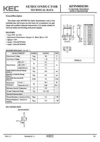
kf5n50d dz.pdf
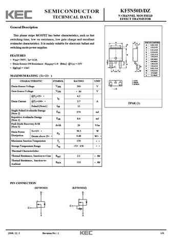
KF5N50D/DZ SEMICONDUCTOR N CHANNEL MOS FIELD TECHNICAL DATA EFFECT TRANSISTOR General Description This planar stripe MOSFET has better characteristics, such as fast switching time, low on resistance, low gate charge and excellent A K DIM MILLIMETERS avalanche characteristics. It is mainly suitable for electronic ballast and L C D _ A 6.60 + 0.20 _ B 6.10 + 0.20 switching mode p... See More ⇒
kf5n50ds.pdf
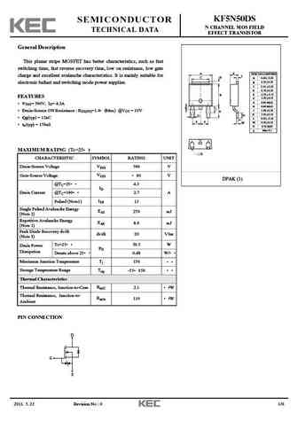
KF5N50DS SEMICONDUCTOR N CHANNEL MOS FIELD TECHNICAL DATA EFFECT TRANSISTOR General Description This planar stripe MOSFET has better characteristics, such as fast switching time, fast reverse recovery time, low on resistance, low gate A K DIM MILLIMETERS charge and excellent avalanche characteristics. It is mainly suitable for L C D _ A 6.60 + 0.20 _ B 6.10 + 0.20 electronic ba... See More ⇒
kf15n50n.pdf
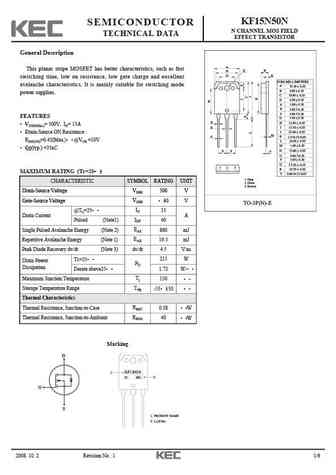
KF15N50N SEMICONDUCTOR N CHANNEL MOS FIELD TECHNICAL DATA EFFECT TRANSISTOR General Description A This planar stripe MOSFET has better characteristics, such as fast Q B N O K switching time, low on resistance, low gate charge and excellent DIM MILLIMETERS avalanche characteristics. It is mainly suitable for switching mode _ A + 15.60 0.20 _ B 4.80 + 0.20 power supplies. _ ... See More ⇒
kf5n50dz-ds.pdf
KF5N50DZ/DS SEMICONDUCTOR N CHANNEL MOS FIELD TECHNICAL DATA EFFECT TRANSISTOR General Description This planar stripe MOSFET has better characteristics, such as fast switching time, fast reverse recovery time, low on resistance, low gate A K DIM MILLIMETERS charge and excellent avalanche characteristics. It is mainly suitable for L C D _ A 6.60 + 0.20 _ B 6.10 + 0.20 electronic... See More ⇒
kf5n50ps-fs.pdf
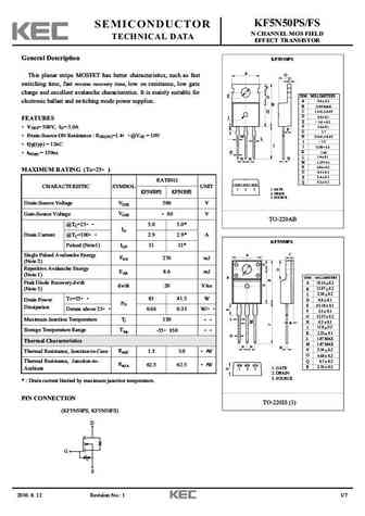
KF5N50PS/FS SEMICONDUCTOR N CHANNEL MOS FIELD TECHNICAL DATA EFFECT TRANSISTOR General Description KF5N50PS A This planar stripe MOSFET has better characteristics, such as fast O C switching time, fast reverse recovery time, low on resistance, low gate F charge and excellent avalanche characteristics. It is mainly suitable for E DIM MILLIMETERS G _ + electronic ballast and swi... See More ⇒
kf5n50dz-iz.pdf
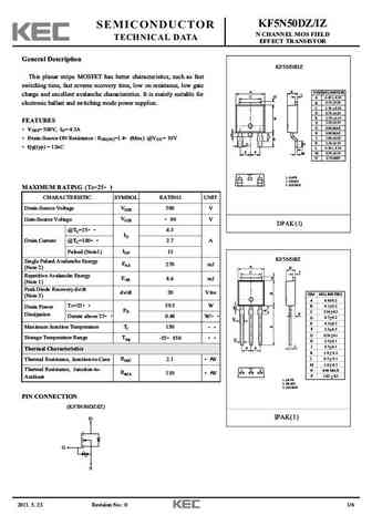
KF5N50DZ/IZ SEMICONDUCTOR N CHANNEL MOS FIELD TECHNICAL DATA EFFECT TRANSISTOR General Description KF5N50DZ This planar stripe MOSFET has better characteristics, such as fast switching time, fast reverse recovery time, low on resistance, low gate A K DIM MILLIMETERS charge and excellent avalanche characteristics. It is mainly suitable for L C D _ A 6.60 + 0.20 _ B 6.10 + 0.20 ... See More ⇒
kf5n50fr kf5n50pr kf5n50ps.pdf
KF5N50PR/FR/PS/FS SEMICONDUCTOR N CHANNEL MOS FIELD TECHNICAL DATA EFFECT TRANSISTOR General Description KF5N50PR, KF5N50PS A This planar stripe MOSFET has better characteristics, such as fast O C switching time, fast reverse recovery time, low on resistance, low gate F charge and excellent avalanche characteristics. It is mainly suitable for E DIM MILLIMETERS G _ + electronic... See More ⇒
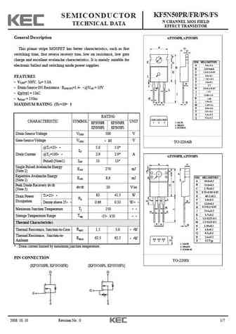
kf5n50fza-fsa.pdf
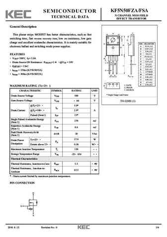
KF5N50FZA/FSA SEMICONDUCTOR N CHANNEL MOS FIELD TECHNICAL DATA EFFECT TRANSISTOR General Description This planar stripe MOSFET has better characteristics, such as fast switching time, fast reverse recovery time, low on resistance, low gate charge and excellent avalanche characteristics. It is mainly suitable for electronic ballast and switching mode power supplies. FEATURES VDSS=... See More ⇒
h05n50.pdf
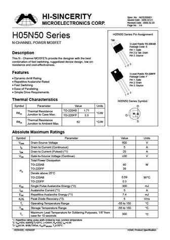
Spec. No. MOS200601 HI-SINCERITY Issued Date 2006.02.01 Revised Date 2006.02.20 MICROELECTRONICS CORP. Page No. 1/4 H05N50 Series Pin Assignment H05N50 Series Tab N-CHANNEL POWER MOSFET 3-Lead Plastic TO-220AB Package Code E Pin 1 Gate Pin 2 & Tab Drain Description Pin 3 Source This N - Channel MOSFETs provide the designer with the best combination of fast switching... See More ⇒
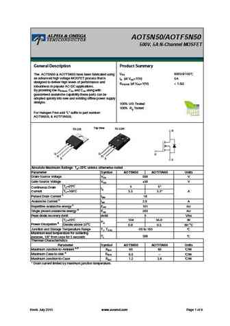
aotf5n50.pdf

AOT5N50/AOTF5N50 500V, 5A N-Channel MOSFET General Description Product Summary VDS 600V@150 The AOT5N50 & AOTF5N50 have been fabricated using an advanced high voltage MOSFET process that is ID (at VGS=10V) 5A designed to deliver high levels of performance and RDS(ON) (at VGS=10V) ... See More ⇒
aot5n50.pdf
AOT5N50/AOTF5N50 500V, 5A N-Channel MOSFET General Description Product Summary VDS 600V@150 The AOT5N50 & AOTF5N50 have been fabricated using an advanced high voltage MOSFET process that is ID (at VGS=10V) 5A designed to deliver high levels of performance and RDS(ON) (at VGS=10V) ... See More ⇒
aotf5n50fd.pdf
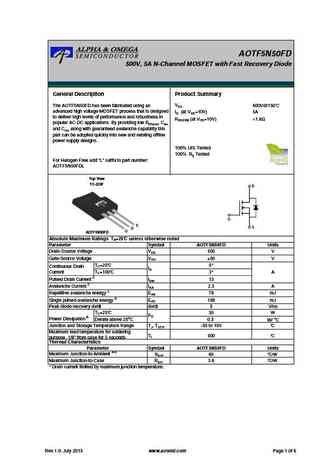
AOTF5N50FD 500V, 5A N-Channel MOSFET with Fast Recovery Diode General Description Product Summary VDS 600V@150 The AOTF5N50FD has been fabricated using an advanced high voltage MOSFET process that is designed ID (at VGS=10V) 5A to deliver high levels of performance and robustness in RDS(ON) (at VGS=10V) ... See More ⇒
aot5n50 aotf5n50.pdf
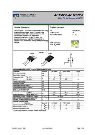
AOT5N50/AOTF5N50 500V, 5A N-Channel MOSFET General Description Product Summary VDS 600V@150 The AOT5N50 & AOTF5N50 have been fabricated using an advanced high voltage MOSFET process that is ID (at VGS=10V) 5A designed to deliver high levels of performance and RDS(ON) (at VGS=10V) ... See More ⇒
aod5n50.pdf
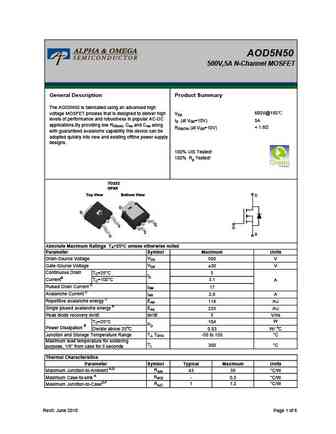
AOD5N50 500V,5A N-Channel MOSFET General Description Product Summary The AOD5N50 is fabricated using an advanced high 600V@150 voltage MOSFET process that is designed to deliver high VDS levels of performance and robustness in popular AC-DC ID (at VGS=10V) 5A applications.By providing low RDS(on), Ciss and Crss along ... See More ⇒
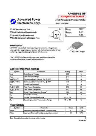
ap05n50h-hf.pdf
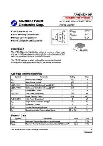
AP05N50H-HF Halogen-Free Product Advanced Power N-CHANNEL ENHANCEMENT MODE Electronics Corp. POWER MOSFET 100% Avalanche Test D BVDSS 500V Fast Switching Characteristic RDS(ON) 1.4 Simple Drive Requirement ID 5.0A G RoHS Compliant & Halogen-Free S G Description D TO-252(H) S The AP05N50 provide high blocking voltage to overcome voltage surge and sag in the toug... See More ⇒
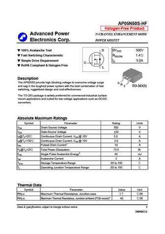
ap05n50ei-hf.pdf
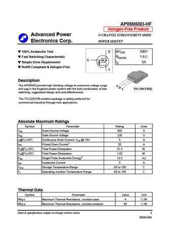
AP05N50EI-HF Halogen-Free Product Advanced Power N-CHANNEL ENHANCEMENT MODE Electronics Corp. POWER MOSFET 100% Avalanche Test BVDSS 500V D Fast Switching Characteristic RDS(ON) 1.6 G Simple Drive Requirement ID 5A RoHS Compliant & Halogen-Free S Description The AP05N50 provide high blocking voltage to overcome voltage surge G D and sag in the toughest power sys... See More ⇒
ap05n50eh.pdf
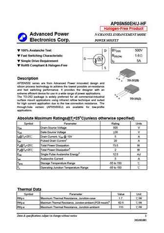
AP05N50EH/J-HF Halogen-Free Product Advanced Power N-CHANNEL ENHANCEMENT MODE Electronics Corp. POWER MOSFET 100% Avalanche Test BVDSS 500V D Fast Switching Characteristic RDS(ON) 1.6 G Simple Drive Requirement ID 5A RoHS Compliant & Halogen-Free S G Description D TO-252(H) S AP05N50E series are from Advanced Power innovated design and silicon process technolo... See More ⇒
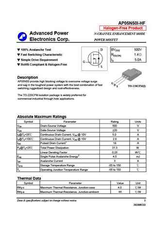
ap05n50eh-hf ap05n50ej-hf.pdf
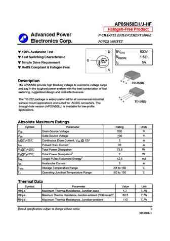
AP05N50EH/J-HF Halogen-Free Product Advanced Power N-CHANNEL ENHANCEMENT MODE Electronics Corp. POWER MOSFET 100% Avalanche Test BVDSS 500V D Fast Switching Characteristic RDS(ON) 1.6 G Simple Drive Requirement ID 5A RoHS Compliant & Halogen-Free S G Description D TO-252(H) S The AP05N50 provide high blocking voltage to overcome voltage surge and sag in the to... See More ⇒
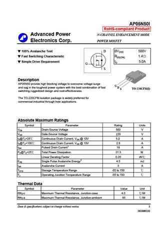
ap05n50p.pdf
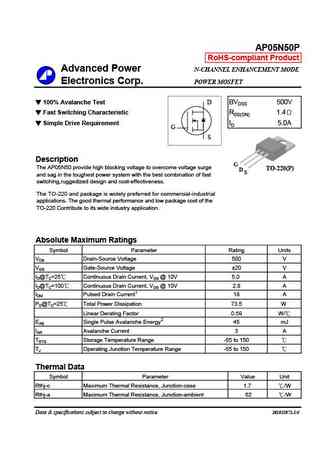
AP05N50P RoHS-compliant Product Advanced Power N-CHANNEL ENHANCEMENT MODE Electronics Corp. POWER MOSFET 100% Avalanche Test D BVDSS 500V Fast Switching Characteristic RDS(ON) 1.4 Simple Drive Requirement ID 5.0A G S Description G The AP05N50 provide high blocking voltage to overcome voltage surge TO-220(P) D S and sag in the toughest power system with the best comb... See More ⇒
ap05n50ib-hf.pdf
AP05N50IB-HF Halogen-Free Product Advanced Power N-CHANNEL ENHANCEMENT MODE Electronics Corp. POWER MOSFET 100% Avalanche Test D BVDSS 500V Fast Switching Characteristic RDS(ON) 1.4 Simple Drive Requirement ID 5.0A G RoHS Compliant & Halogen-Free S Description AP05N50 provide high blocking voltage to overcome voltage surge and sag in the toughest power system with ... See More ⇒
ap05n50s-hf.pdf
AP05N50S-HF Halogen-Free Product Advanced Power N-CHANNEL ENHANCEMENT MODE Electronics Corp. POWER MOSFET 100% Avalanche Test D BVDSS 500V Fast Switching Characteristic RDS(ON) 1.4 Simple Drive Requirement ID 5.0A G RoHS Compliant & Halogen-Free S Description The AP05N50 provide high blocking voltage to overcome voltage surge G D and sag in the toughest power sys... See More ⇒
ap05n50i.pdf
AP05N50I RoHS-compliant Product Advanced Power N-CHANNEL ENHANCEMENT MODE Electronics Corp. POWER MOSFET 100% Avalanche Test D BVDSS 500V Fast Switching Characteristic RDS(ON) 1.4 Simple Drive Requirement ID 5.0A G S Description AP05N50 provide high blocking voltage to overcome voltage surge G and sag in the toughest power system with the best combination of fast D TO... See More ⇒
ap05n50ej.pdf

AP05N50EH/J-HF Halogen-Free Product Advanced Power N-CHANNEL ENHANCEMENT MODE Electronics Corp. POWER MOSFET 100% Avalanche Test BVDSS 500V D Fast Switching Characteristic RDS(ON) 1.6 G Simple Drive Requirement ID 5A RoHS Compliant & Halogen-Free S G Description D TO-252(H) S AP05N50E series are from Advanced Power innovated design and silicon process technolo... See More ⇒
ap05n50i-hf.pdf
AP05N50I-HF Halogen-Free Product Advanced Power N-CHANNEL ENHANCEMENT MODE Electronics Corp. POWER MOSFET 100% Avalanche Test D BVDSS 500V Fast Switching Characteristic RDS(ON) 1.4 Simple Drive Requirement ID 5.0A G RoHS Compliant & Halogen-Free S Description AP05N50 provide high blocking voltage to overcome voltage surge G and sag in the toughest power system wit... See More ⇒
sif5n50c 1.pdf
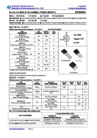
Shenzhen SI Semiconductors Co., LTD. Product Specification Shenzhen SI Semiconductors Co., LTD. Product Specification Shenzhen SI Semiconductors Co., LTD. Product Specification Shenzhen SI Semiconductors Co., LTD. Product Specification N- MOS / N-CHANNEL POWER MOSFET SIF5N50C N- MOS / N-CHANNEL POWER MOSFET SIF5N50C N- MOS / N-CHANN... See More ⇒
sif5n50c.pdf
Shenzhen SI Semiconductors Co., LTD. Product Specification Shenzhen SI Semiconductors Co., LTD. Product Specification Shenzhen SI Semiconductors Co., LTD. Product Specification Shenzhen SI Semiconductors Co., LTD. Product Specification N- MOS / N-CHANNEL POWER MOSFET SIF5N50C N- MOS / N-CHANNEL POWER MOSFET SIF5N50C N- MOS / N-CHANN... See More ⇒
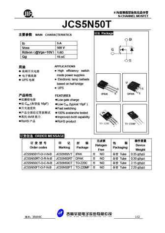
jcs5n50vt jcs5n50rt jcs5n50ct jcs5n50ft.pdf
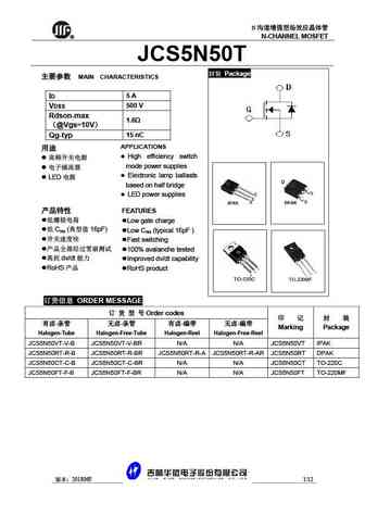
N R N-CHANNEL MOSFET JCS5N50T Package MAIN CHARACTERISTICS 5 A ID 500 V VDSS Rdson-max 1.6 @Vgs=10V 15 nC Qg-typ APPLICATIONS High efficiency switch mode power supplies Electronic lamp ballasts LED based on half bridge ... See More ⇒
jcs5n50vc jcs5n50rc jcs5n50cc jcs5n50fc.pdf
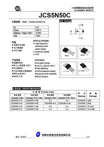
N R N-CHANNEL MOSFET JCS5N50C Package MAIN CHARACTERISTICS 5 A ID 500 V VDSS Rdson Vgs=10V 1.45 14nC Qg APPLICATIONS High frequency switching mode power supply UPS Electronic ballast UPS FEATURES ... See More ⇒
mtn5n50fp.pdf
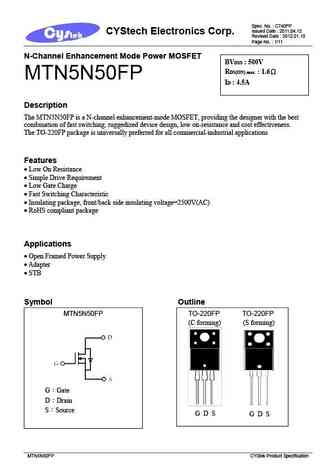
Spec. No. C740FP Issued Date 2011.04.12 CYStech Electronics Corp. Revised Date 2012.01.10 Page No. 1/11 N-Channel Enhancement Mode Power MOSFET BVDSS 500V RDS(ON) max. 1.6 MTN5N50FP ID 4.5A Description The MTN5N50FP is a N-channel enhancement-mode MOSFET, providing the designer with the best combination of fast switching, ruggedized device design, low on-r... See More ⇒
mtn5n50j3.pdf
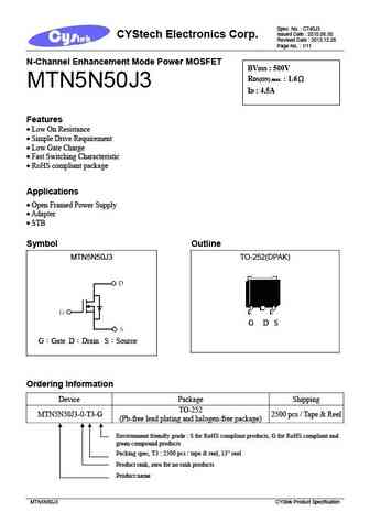
Spec. No. C740J3 Issued Date 2010.06.30 CYStech Electronics Corp. Revised Date 2013.12.26 Page No. 1/11 N-Channel Enhancement Mode Power MOSFET BVDSS 500V RDS(ON) max. 1.6 MTN5N50J3 ID 4.5A Features Low On Resistance Simple Drive Requirement Low Gate Charge Fast Switching Characteristic RoHS compliant package Applications ... See More ⇒
mtn15n50fp.pdf
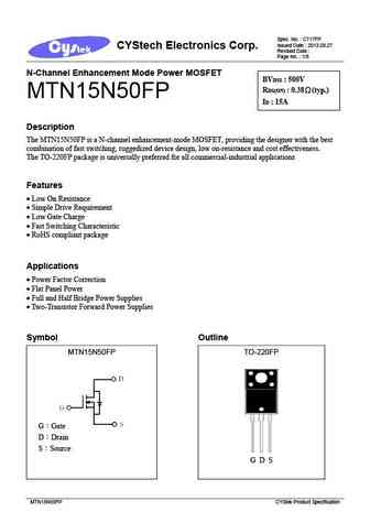
Spec. No. C717FP Issued Date 2013.08.27 CYStech Electronics Corp. Revised Date Page No. 1/8 N-Channel Enhancement Mode Power MOSFET BVDSS 500V RDS(ON) 0.38 (typ.) MTN15N50FP ID 15A Description The MTN15N50FP is a N-channel enhancement-mode MOSFET, providing the designer with the best combination of fast switching, ruggedized device design, low on-resistance... See More ⇒
mtn5n50i3.pdf
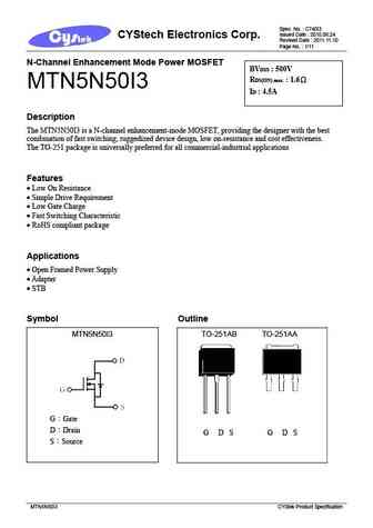
Spec. No. C740I3 Issued Date 2010.06.24 CYStech Electronics Corp. Revised Date 2011.11.10 Page No. 1/11 N-Channel Enhancement Mode Power MOSFET BVDSS 500V RDS(ON) max. 1.6 MTN5N50I3 ID 4.5A Description The MTN5N50I3 is a N-channel enhancement-mode MOSFET, providing the designer with the best combination of fast switching, ruggedized device design, low on-r... See More ⇒
mtn5n50e3.pdf
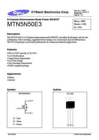
Spec. No. C740E3 Issued Date 2009.09.14 CYStech Electronics Corp. Revised Date Page No. 1/8 N-Channel Enhancement Mode Power MOSFET BVDSS 500V RDS(ON) 1.5 MTN5N50E3 ID 4.5A Description The MTN5N50E3 is a N-channel enhancement-mode MOSFET, providing the designer with the best combination of fast switching, ruggedized device design, low on-resistance and cos... See More ⇒
mtn15n50f3.pdf

Spec. No. C717F3 Issued Date 2010.08.03 CYStech Electronics Corp. Revised Date Page No. 1/11 N-Channel Enhancement Mode Power MOSFET BVDSS 500V RDS(ON) 0.38 (typ.) MTN15N50F3 ID 15A Description The MTN15N50F3 is a N-channel enhancement-mode MOSFET, providing the designer with the best combination of fast switching, ruggedized device design, low on-resistanc... See More ⇒
mtn15n50e3.pdf
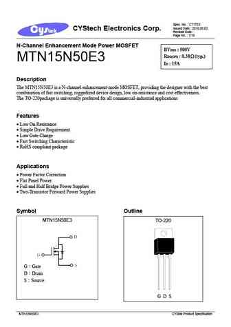
Spec. No. C717E3 Issued Date 2010.08.03 CYStech Electronics Corp. Revised Date Page No. 1/10 N-Channel Enhancement Mode Power MOSFET BVDSS 500V RDS(ON) 0.38 (typ.) MTN15N50E3 ID 15A Description The MTN15N50E3 is a N-channel enhancement-mode MOSFET, providing the designer with the best combination of fast switching, ruggedized device design, low on-resistanc... See More ⇒
g5n50t g5n50f g5n50j g5n50k.pdf
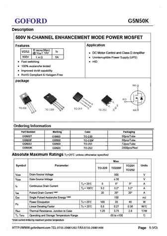
G5N50K GOFORD Description 500V N-CHANNEL ENHANCEMENT MODE POWER MOSFET Application Features R DS(ON)(Max) I VDSS D .@ VGS = 10V DC Motor Control and Class D Amplifier 500V 5A Uninterruptible Power Supply (UPS) 1.4 Fast switching HID 100% avalanche tested Improved dv/dt capability RoHS Compliant & Halogen-Free Package Ordering Informa... See More ⇒
sdf05n50 sdp05n50.pdf
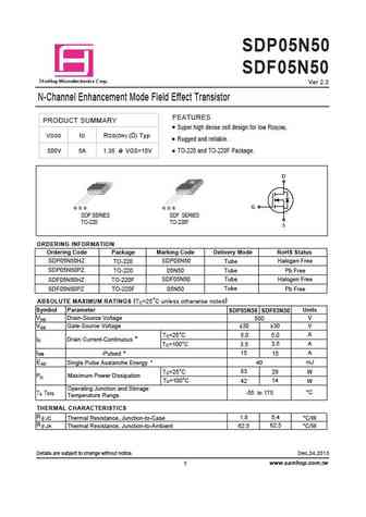
SDP05N50 SDF05N50 a S mHop Microelectronics C orp. Ver 2.3 N-Channel Enhancement Mode Field Effect Transistor FEATURES PRODUCT SUMMARY Super high dense cell design for low RDS(ON). VDSS ID RDS(ON) ( ) Typ Rugged and reliable. 500V 5A 1.35 @ VGS=10V TO-220 and TO-220F Package. D G G D S G D S SDP SERIES SDF SERIES TO-220 TO-220F S ORDERING INFORMATION Ordering Code Package Ma... See More ⇒
ssf5n50d.pdf
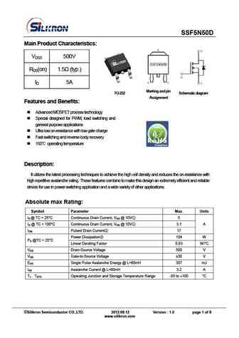
SSF5N50D Main Product Characteristics VDSS 500V RDS(on) 1.5 (typ.) ID 5A TO-252 Marking a nd p in S che ma ti c di ag r a m Assignment Features and Benefits Advanced MOSFET process technology Special designed for PWM, load switching and general purpose applications Ultra low on-resistance with low gate charge Fast switching and reverse body recovery... See More ⇒
fsw25n50a.pdf
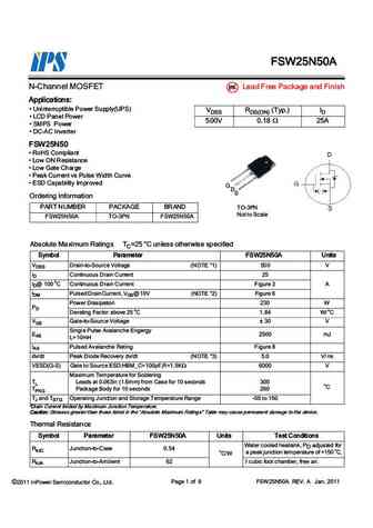
FSW25N50A N-Channel MOSFET Pb Lead Free Package and Finish Applications Uninterruptible Power Supply(UPS) VDSS RDS(ON) (Typ.) ID LCD Panel Power 500V 0.18 25A SMPS Power DC-AC Inverter FSW25N50 RoHS Compliant Low ON Resistance Low Gate Charge Peak Current vs Pulse Width Curve ESD Capability Improved G D S Ordering Information PART NU... See More ⇒
bri5n50.pdf
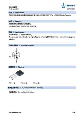
BRI5N50 Rev.D Nov.-2015 DATA SHEET / Descriptions TO-251 N MOS N-CHANNEL MOSFET in a TO-251 Plastic Package. / Features , , Low gate charge, low crss, fast switching. / Applications DC/DC These devices are well suited for high efficiency sw... See More ⇒
brd5n50.pdf
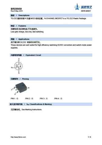
BRD5N50 Rev.D May.-2016 DATA SHEET / Descriptions TO-252 N MOS N-CHANNEL MOSFET in a TO-252 Plastic Package. / Features , , Low gate charge, low crss, fast switching. / Applications DC/DC These devices are well suited for high efficiency switching... See More ⇒
brf5n50.pdf
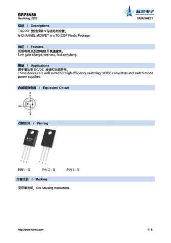
BRF5N50 Rev.A Aug.-2022 DATA SHEET / Descriptions TO-220F N N-CHANNEL MOSFET in a TO-220F Plastic Package. / Features , , Low gate charge, low crss, fast switching. / Applications DC/DC , These devices are well suited for high efficiency... See More ⇒
brfl15n50.pdf
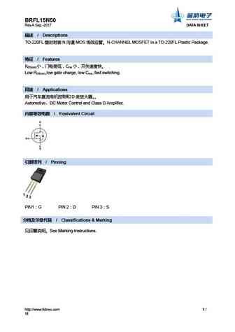
BRFL15N50 Rev.A Sep.-2017 DATA SHEET / Descriptions TO-220FL N MOS N-CHANNEL MOSFET in a TO-220FL Plastic Package. / Features R C DS(on) rss Low RDS(on),low gate charge, low Crss, fast switching. / Applications D Automoti... See More ⇒
cs15n50 a8r.pdf
Silicon N-Channel Power MOSFET R CS15N50 A8R General Description VDSS 500 V CS15N50 A8R, the silicon N-channel Enhanced ID 15 A PD(TC=25 ) 180 W VDMOSFETs, is obtained by the self-aligned planar Technology RDS(ON)Typ 0.3 which reduce the conduction loss, improve switching performance and enhance the avalanche energy. The transistor can be used in various pow... See More ⇒
cs15n50f a9r.pdf

Silicon N-Channel Power MOSFET R CS15N50F A9R General Description VDSS 500 V CS15N50F A9R, the silicon N-channel Enhanced VDMOSFETs, ID 15 A PD(TC=25 ) 70 W is obtained by the self-aligned planar Technology which reduce RDS(ON)Typ 0.3 the conduction loss, improve switching performance and enhance the avalanche energy. The transistor can be used in various ... See More ⇒
cs5n50.pdf
CS5N50 N PD TC=25 74 W 0.59 W/ ID VGS=10V,TC=25 5.0 A ID VGS=10V,TC=100 3.2 A IDM 20 A VGS 20 V Tjm +150 Tstg -55 +150 RthJC 1.7 /W BVDSS VGS=0V,ID=0.25mA 500 V RDS on VGS=10V,ID=3A 1.4 ... See More ⇒
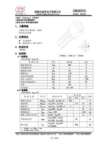
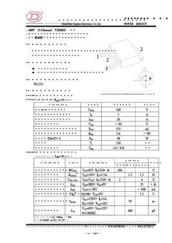
cm5n50 to220a.pdf

R C55 MN0 www.jdsemi.cn ShenZhen Jingdao Electronic Co.,Ltd. POWER MOSFET 500V N-Channel VDMOS RoHS 1 2 3 T... See More ⇒
cm15n50.pdf
R C1N0 M55 www.jdsemi.cn ShenZhen Jingdao Electronic Co.,Ltd. POWER MOSFET 500V N-Channel VDMOS RoHS 1 2 3 ... See More ⇒
cm5n50c.pdf
R CM5N50C www.jdsemi.cn ShenZhen Jingdao Electronic Co.,Ltd. POWER MOSFET 500V N-Channel VDMOS RoHS ... See More ⇒
ftk5n50d.pdf
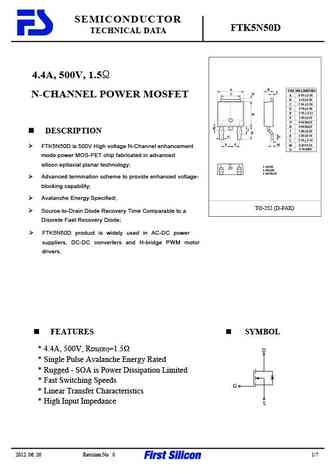
SEMICONDUCTOR FTK5N50D TECHNICAL DATA 4.4A, 500V, 1.5 A K DIM MILLIMETERS L C D _ A 6 60 + 0 20 N-CHANNEL POWER MOSFET _ B 6 10 + 0 20 _ C 5 34 + 0 30 _ D 0 70 + 0 20 _ E 2 70 0 15 + B _ + F 2 30 0 10 G 0 96 MAX H 0 90 MAX H J _ J 1 80 + 0 20 DESCRIPTION E _ K 2 30 + 0 10 G N _ L 0 50 0 10 + F F M _ + M 0 50 0 10 FTK5N50D is 500V High voltage N-Chan... See More ⇒
d5n50 b5n50.pdf
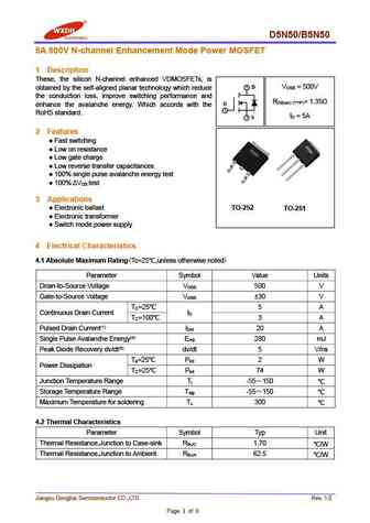
D5N50/B5N50 5A 500V N-channel Enhancement Mode Power MOSFET 1 Description These, the silicon N-channel enhanced VDMOSFETs, is 2 D V = 500V DSS obtained by the self-aligned planar technology which reduce the conduction loss, improve switching performance and R = 1.35 DS(on) (TYP) G enhance the avalanche energy. Which accords with the 1 RoHS standard. I = 5A 3 S D 2 ... See More ⇒
kdb15n50.pdf
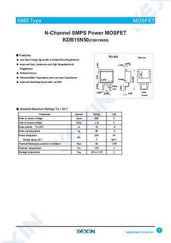
SMD Type MOSFET N-Channel SMPS Power MOSFET KDB15N50(FDB15N50) Features TO-263 Unit mm Low Gate Charge Qg results in Simple Drive Requirement +0.2 4.57-0.2 +0.1 Improved Gate, Avalanche and High Reapplied dv/dt 1.27-0.1 Ruggedness Reduced rDS(ON) Reduced Miller Capacitance and Low Input Capacitance +0.1 0.1max 1.27-0.1 Improved Switching Speed with Low EMI +0.1 0.81-0.1 2.... See More ⇒
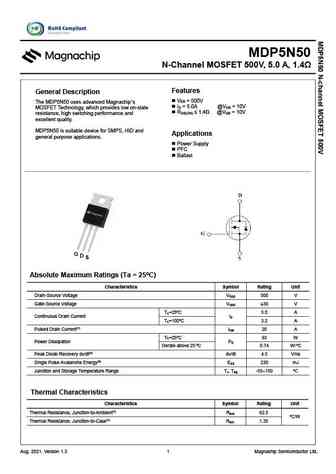
mdd5n50frh.pdf
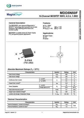
MDD5N50F N-Channel MOSFET 500V, 4.2 A, 1.55 General Description Features The MDD5N50F uses advanced Magnachip s V = 500V DS MOSFET Technology, which provides low on-state I = 4.2A @V = 10V D GS resistance, high switching performance and RDS(ON) 1.5 @VGS = 10V excellent quality. MDD5N50F is suitable device for Power Supply, Applications PFC and gen... See More ⇒
mdd5n50zrh.pdf
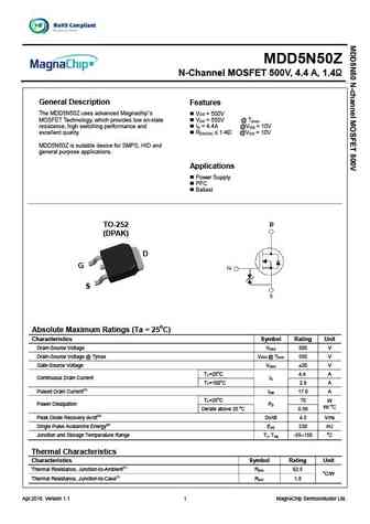
MDD5N50Z N-Channel MOSFET 500V, 4.4 A, 1.4 General Description Features The MDD5N50Z uses advanced Magnachip s V = 500V DS MOSFET Technology, which provides low on-state VDS = 550V @ Tjmax resistance, high switching performance and I = 4.4A @V = 10V D GS excellent quality. R 1.4 @V = 10V DS(ON) GS MDD5N50Z is suitable device for SMPS, HID and general pur... See More ⇒
mdf5n50zth mdp5n50zth.pdf
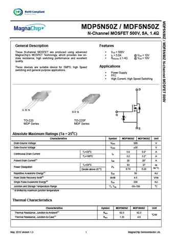
MDP5N50Z / MDF5N50Z N-Channel MOSFET 500V, 5A, 1.4 General Description Features These N-channel MOSFET are produced using advanced V = 500V DS MagnaChip s MOSFET Technology, which provides low on- I = 5.0A @ V = 10V D GS state resistance, high switching performance and excellent R 1.4 @ V = 10V DS(ON) GS quality. Applications These devices are suitable device fo... See More ⇒
mdf5n50fth mdp5n50fth.pdf
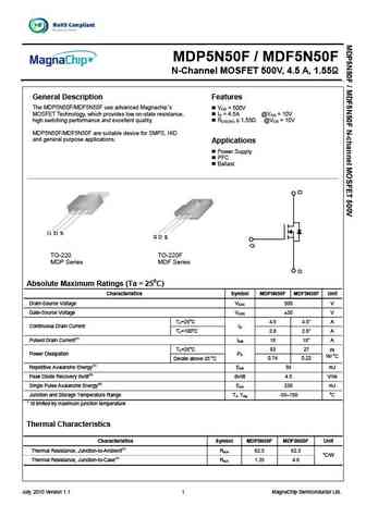
MDP5N50F / MDF5N50F N-Channel MOSFET 500V, 4.5 A, 1.55 General Description Features The MDP5N50F/MDF5N50F use advanced Magnachip s V = 500V DS MOSFET Technology, which provides low on-state resistance, I = 4.5A @V = 10V D GS high switching performance and excellent quality. RDS(ON) 1.55 @VGS = 10V MDP5N50F/MDF5N50F are suitable device for SMPS, HID and genera... See More ⇒
mdd5n50rh.pdf

MDD5N50 N-Channel MOSFET 500V, 4.4 A, 1.4 General Description Features The MDD5N50 uses advanced Magnachip s V = 500V DS MOSFET Technology, which provides low on-state I = 4.4A @V = 10V D GS resistance, high switching performance and RDS(ON) 1.4 @VGS = 10V excellent quality. MDD5N50 is suitable device for SMPS, Ballast and general purpose applicatio... See More ⇒
mdf5n50fbth.pdf
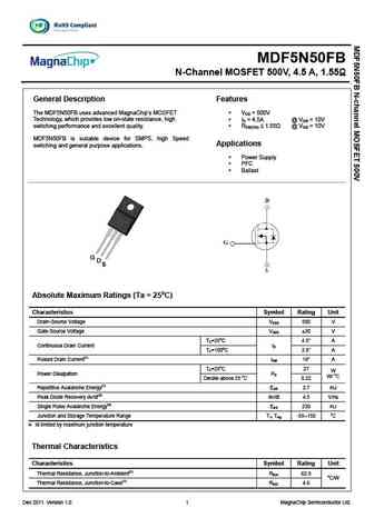
MDF5N50FB N-Channel MOSFET 500V, 4.5 A, 1.55 General Description Features The MDF5N50FB uses advanced MagnaChip s MOSFET VDS = 500V Technology, which provides low on-state resistance, high ID = 4.5A @ VGS = 10V switching performance and excellent quality. RDS(ON) 1.55 @ VGS = 10V MDF5N50FB is suitable device for SMPS, high Speed Applications switching ... See More ⇒
mdis5n50th.pdf
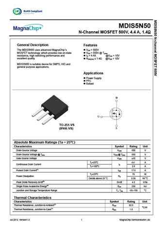
MDIS5N50 N-Channel MOSFET 500V, 4.4 A, 1.4 General Description Features The MDIS5N50 uses advanced MagnaChip s VDS = 500V MOSFET technology, which provides low on-state VDS = 550V @ Tjmax resistance, high switching performance and ID = 4.4A @VGS = 10V excellent quality. RDS(ON) 1.4 @VGS = 10V MDIS5N50 is suitable device for SMPS, HID and general ... See More ⇒
mdf5n50bth mdp5n50bth.pdf
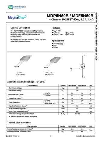
MDP5N50B / MDF5N50B N-Channel MOSFET 500V, 5.0 A, 1.4 General Description Features The MDP/F5N50B uses advanced Magnachip s VDS = 500V MOSFET Technology, which provides low on-state ID = 5.0A @VGS = 10V resistance, high switching performance and RDS(ON) 1.4 @VGS = 10V excellent quality. MDP/F5N50B is suitable device for SMPS, HID and Applications general purpose... See More ⇒
mdp5n50th.pdf
MDP5N50 N-Channel MOSFET 500V, 5.0 A, 1.4 Features General Description V = 500V DS The MDP5N50 uses advanced Magnachip s I = 5.0A @V = 10V D GS MOSFET Technology, which provides low on-state R 1.4 @V = 10V DS(ON) GS resistance, high switching performance and excellent quality. MDP5N50 is suitable device for SMPS, HID and Applications gener... See More ⇒
ms15n50.pdf
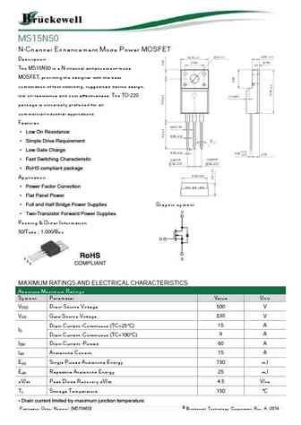
MS15N50 N-Channel Enhancement Mode Power MOSFET Description The MS15N50 is a N-channel enhancement-mode MOSFET, providing the designer with the best combination of fast switching, ruggedized device design, low on-resistance and cost effectiveness. The TO-220 package is universally preferred for all commercial-industrial applications Features Low On Resistance Simpl... See More ⇒
msq5n50.pdf
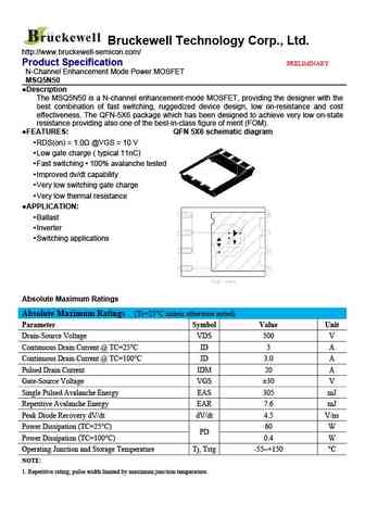
Bruckewell Technology Corp., Ltd. http //www.bruckewell-semicon.com/ Product Specification PRELIMINARY N-Channel Enhancement Mode Power MOSFET MSQ5N50 Description The MSQ5N50 is a N-channel enhancement-mode MOSFET, providing the designer with the best combination of fast switching, ruggedized device design, low on-resistance and cost effectiveness. The QFN-5X6 package which ... See More ⇒
ms5n50-a.pdf
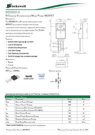
MS5N50-A N-Channel Enhancement Mode Power MOSFET Description The MS5N50-A is a N-channel enhancement-mode MOSFET, providing the designer with the best combination of fast switching, ruggedized device design, low on-resistance and cost effectiveness. The TO-220 package is universally preferred for all commercial-industrial applications Features BVDSS=550V typically @ Tj=1... See More ⇒
msf5n50.pdf
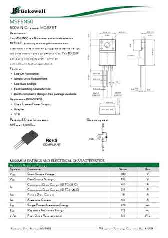
MSF5N50 500V N-Channel MOSFET Description The MSF5N50 is a N-channel enhancement-mode MOSFET , providing the designer with the best combination of fast switching, ruggedized device design, low on-resistance and cost effectiveness. The TO-220F package is universally preferred for all commercial-industrial applications Features Low On Resistance Simple Drive Requirem... See More ⇒
msu5n50.pdf
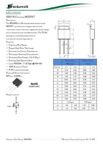
MSU5N50 500V N-Channel MOSFET Description The MSU5N50 is a N-channel enhancement-mode MOSFET , providing the designer with the best combination of fast switching, ruggedized device design, low on-resistance and cost effectiveness. The TO-251 package is universally preferred for all commercial-industrial applications Features Originative New Design Rugged Gate Oxide... See More ⇒
ms5n50.pdf
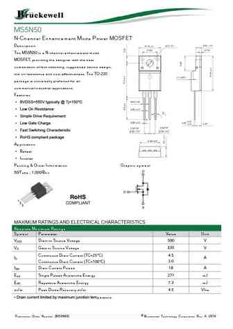
MS5N50 N-Channel Enhancement Mode Power MOSFET Description The MS5N50 is a N-channel enhancement-mode MOSFET, providing the designer with the best combination of fast switching, ruggedized device design, low on-resistance and cost effectiveness. The TO-220 package is universally preferred for all commercial-industrial applications Features BVDSS=550V typically @ Tj=150 ... See More ⇒
wfp5n50.pdf
WFP5N50 WFP5N50 WFP5N50 WFP5N50 Silicon N-Channel MOSFET Silicon N-Channel MOSFET Silicon N-Channel MOSFET Silicon N-Channel MOSFET Features 5A,500V,RDS(on)(Max1.6 )@VGS=10V Ultra-low Gate Charge(Typical 32nC) Fast Switching Capability 100%Avalanche Tested Maximum Junction Temperature Range(150 ) General Description This Power MO SFET is pro du ced using Wi... See More ⇒
sfp5n50.pdf
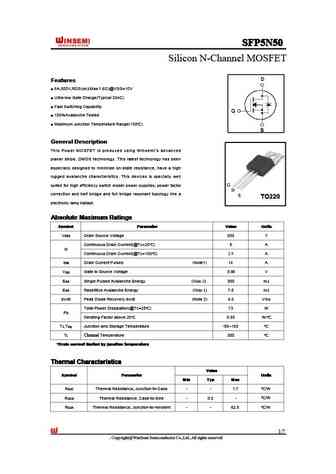
SFP5N50 SFP5N50 SFP5N50 SFP5N50 Silicon N-Channel MOSFET Features Features Features Features 5A,500V,RDS(on)(Max 1.6 )@VGS=10V Ultra-low Gate Charge(Typical 32nC) Fast Switching Capability 100%Avalanche Tested Maximum Junction Temperature Range(150 ) General Description General Description General Description General Description This Power MOSFET is prod... See More ⇒
wfu5n50.pdf
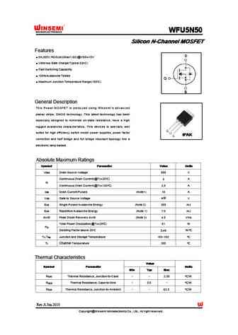
WFU5N50 WFU5N50 WFU5N50 WFU5N50 Silicon N-Channel MOSFET Silicon N-Channel MOSFET Silicon N-Channel MOSFET Silicon N-Channel MOSFET Features 5A,500V,RDS(on)(Max1.6 )@VGS=10V Ultra-low Gate Charge(Typical 32nC) Fast Switching Capability 100%Avalanche Tested Maximum Junction Temperature Range(150 ) General Description This Power MO SFET is pro du ced using Wi... See More ⇒
wfd5n50.pdf
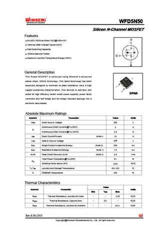
WFD5N50 WFD5N50 WFD5N50 WFD5N50 Silicon N-Channel MOSFET Silicon N-Channel MOSFET Silicon N-Channel MOSFET Silicon N-Channel MOSFET Features 5A,500V,RDS(on)(Max1.6 )@VGS=10V Ultra-low Gate Charge(Typical 32nC) Fast Switching Capability 100%Avalanche Tested Maximum Junction Temperature Range(150 ) General Description This Power MO SFET is pro du ced using Wi... See More ⇒
af15n50.pdf
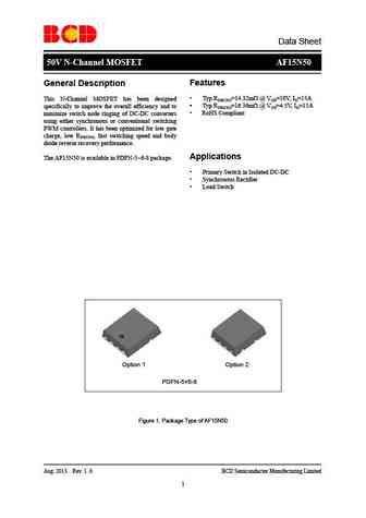
Data Sheet 50V N-Channel MOSFET AF15N50 Features General Description Typ RDS(ON)=14.32m @ VGS=10V, ID=15A This N-Channel MOSFET has been designed Typ RDS(ON)=16.36m @ VGS=4.5V, ID=15A specifically to improve the overall efficiency and to RoHS Compliant minimize switch node ringing of DC-DC converters using either synchronous or conventional switching PWM ... See More ⇒
bl25n50-w bl25n50-f.pdf
BL25N50 Power MOSFET Power MOSFET Power MOSFET Power MOSFET 1 Description BL25N50, the silicon N-channel Enhanced MOSFETs, is obtained by advanced MOSFET technology which reduce the conduction loss, improve switching performance and enhance the avalanche energy. The transistor is suitable device for SMPS, high speed switching and general purpose applicati... See More ⇒
bl15n50-p bl15n50-a bl15n50-f.pdf
BL15N50-APF Power MOSFET 1.Description Step-Down Converter BL15N50-APF, the silicon N-channel , Enhanced MOSFETs, is obtained by advanced MOSFET technology which reduce the conduction loss, improve switching performance and enhance the avalanche energy. The transistor is suitable device for SMPS, high speed switching and general purpose applications. KEY CHARACTERISTICS... See More ⇒
bl5n50-p bl5n50-a bl5n50-u bl5n50-d.pdf
BL5N50 Power MOSFET 1 Description Step-Down Converter BL5N50, the silicon N-channel Enhanced , MOSFETs, is obtained by advanced MOSFET technology which reduce the conduction loss, improve switching performance and enhance the avalanche energy. The transistor is suitable device for SMPS, high speed switching and general purpose applications. KEY CHARACTERISTICS Para... See More ⇒
cs55n50.pdf
CS55N50 N-Channel Trench Power MOSFET General Description The CS55N50 is N-channel MOS Field Effect Transistor designed for high current switching applications. Rugged EAS capability and ultra low RDS(ON) is suitable for PWM, load switching . Features VDS=55V; ID=105A@ VGS=10V; RDS(ON)... See More ⇒
hy5n50t.pdf
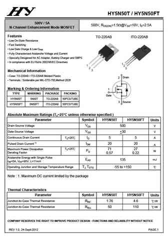
HY5N50T / HY5N50FT 500V / 5A 500V, RDS(ON)=1.5W@VGS=10V, ID=2.5A N-Channel Enhancement Mode MOSFET Features TO-220AB ITO-220AB Low On-State Resistance Fast Switching Low Gate Charge & Low CRSS Fully Characterized Avalanche Voltage and Current Specially Desigened for AC Adapter, Battery Charger and SMPS In compliance with EU RoHs 2002/95/EC Directives 1 ... See More ⇒
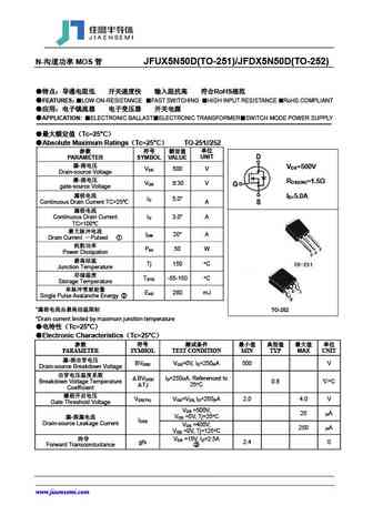
jfux5n50d jfdx5n50d.pdf
N- MOS JFUX5N50D(TO-251)/JFDX5N50D(TO-252) RoHS FEATURES LOW ON-RESISTANCE FAST SWITCHING HIGH INPUT RESISTANCE RoHS COMPLIANT APPLICATION ELECTRONIC BALLAST ELECTRONIC TRANSFORMER SWITCH MODE POWER SUPPLY ... See More ⇒
jfam25n50e.pdf
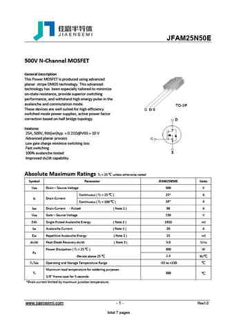
JFAM25N50E 500V N-Channel MOSFET General Description This Power MOSFET is produced using advanced planar stripe DMOS technology. This advanced technology has been especially tailored to minimize on-state resistance, provide superior switching performance, and withstand high energy pulse in the avalanche and commutation mode. These devices are well suited for high efficiency ... See More ⇒
sld5n50s2 slu5n50s2.pdf
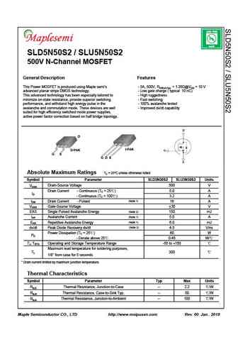
LEAD FREE Pb RoHS SLD5N50S2 / SLU5N50S2 500V N-Channel MOSFET General Description Features This Power MOSFET is produced using Maple semi s - 5A, 500V, RDS(on) typ. = 1.35 @VGS = 10 V ( ) yp advanced planar stripe DMOS technology. - Low gate charge ( typical 10 nC) This advanced technology has been especially tailored to - High ruggedness minimize on-state resistance, provide super... See More ⇒
slp5n50s slf5n50s.pdf
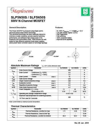
LEAD FREE Pb RoHS SLP5N50S / SLF5N50S 500V N-Channel MOSFET General Description Features This Power MOSFET is produced using Maple semi s - 5A, 500V, RDS(on) typ. = 1.12 @VGS = 10 V advanced planar stripe DMOS technology. - Low gate charge ( typical 22 nC) This advanced technology has been especially tailored to - High ruggedness minimize on-state resistance, provide superi... See More ⇒
ptp15n50 pta15n50.pdf
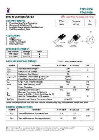
PTP15N50 PTA15N50 500V N-Channel MOSFET General Features BVDSS RDS(ON),typ. ID Proprietary New Planar Technology 500V 0.33 15A RDS(ON),typ.=0.33 @VGS=10V Low Gate Charge Minimize Switching Loss Fast Recovery Body Diode Applications Adaptor TV Main Power SMPS Power Supply LCD Panel Power Ordering Information Part Number Package Bran... See More ⇒
pta25n50.pdf
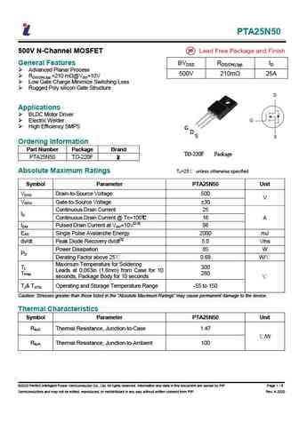
PTA25N50 500V N-Channel MOSFET General Features BVDSS RDS(ON),typ. ID Advanced Planar Process 500V 210m 25A RDS(ON),typ.=210 m @VGS=10V Low Gate Charge Minimize Switching Loss Rugged Poly silicon Gate Structure Applications BLDC Motor Driver Electric Welder High Efficiency SMPS G D S Ordering Information Part Number Package Brand TO-220F Package P... See More ⇒
swmn15n50d.pdf
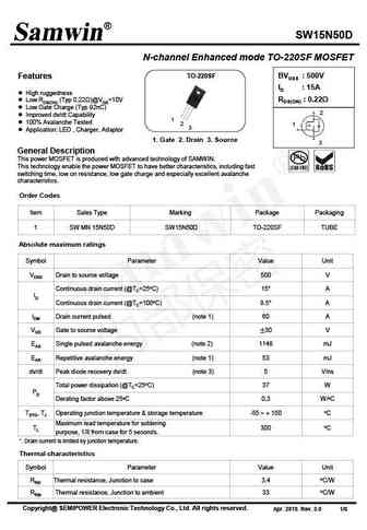
SW15N50D N-channel Enhanced mode TO-220SF MOSFET TO-220SF BVDSS 500V Features ID 15A High ruggedness RDS(ON) 0.22 Low RDS(ON) (Typ 0.22 )@VGS=10V Low Gate Charge (Typ 92nC) 2 Improved dv/dt Capability 1 100% Avalanche Tested 2 1 3 Application LED , Charger, Adaptor 1. Gate 2. Drain 3. Source 3 General Description This... See More ⇒
swf15n50.pdf
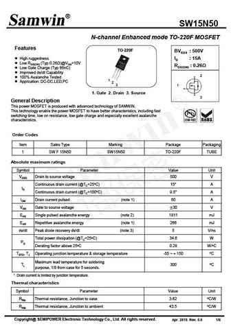
SW15N50 N-channel Enhanced mode TO-220F MOSFET Features TO-220F BVDSS 500V High ruggedness ID 15A Low RDS(ON) (Typ 0.26 )@VGS=10V RDS(ON) 0.26 Low Gate Charge (Typ 66nC) Improved dv/dt Capability 2 100% Avalanche Tested 1 Application DC-DC,LED,PC 2 3 1 1. Gate 2. Drain 3. Source 3 General Description This power MOSFET is... See More ⇒
swf15n50da.pdf
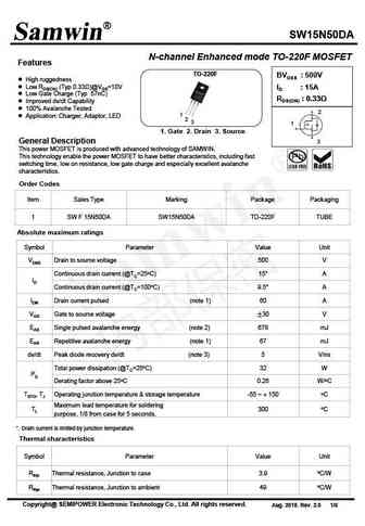
SW15N50DA N-channel Enhanced mode TO-220F MOSFET Features TO-220F BVDSS 500V High ruggedness Low RDS(ON) (Typ 0.33 )@VGS=10V ID 15A Low Gate Charge (Typ 57nC) RDS(ON) 0.33 Improved dv/dt Capability 100% Avalanche Tested 2 1 Application Charger, Adaptor, LED 2 3 1 1. Gate 2. Drain 3. Source General Description 3 This p... See More ⇒
hfs5n50s.pdf
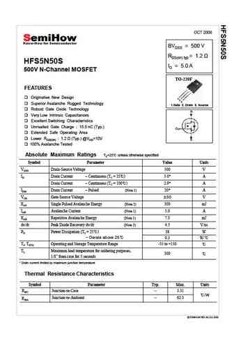
OCT 2008 BVDSS = 500 V RDS(on) typ HFS5N50S ID = 5.0 A 500V N-Channel MOSFET TO-220F FEATURES Originative New Design 1 2 3 Superior Avalanche Rugged Technology 1.Gate 2. Drain 3. Source Robust Gate Oxide Technology Very Low Intrinsic Capacitances Excellent Switching Characteristics Unrivalled Gate Charge 15.5 nC (Typ.) Extended Safe Operating Area ... See More ⇒
hfs5n50u.pdf
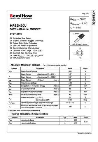
May 2012 BVDSS = 500 V RDS(on) typ HFS5N50U ID = 5.0 A 500V N-Channel MOSFET TO-220F FEATURES Originative New Design Superior Avalanche Rugged Technology 1 2 3 Robust Gate Oxide Technology 1.Gate 2. Drain 3. Source Very Low Intrinsic Capacitances Excellent Switching Characteristics Unrivalled Gate Charge 13 nC (Typ.) Extended Safe Operating Area L... See More ⇒
hfd5n50s.pdf
OCT 2009 BVDSS = 500 V RDS(on) typ HFD5N50S / HFU5N50S ID = 4.0 A 500V N-Channel MOSFET D-PAK I-PAK 2 FEATURES 1 1 3 2 3 Originative New Design HFD5N50S HFU5N50S Superior Avalanche Rugged Technology 1.Gate 2. Drain 3. Source Robust Gate Oxide Technology Very Low Intrinsic Capacitances Excellent Switching Characteristics Unrivalled Gate Charge 15.5 nC ... See More ⇒
hfd5n50s hfu5n50s.pdf

OCT 2009 BVDSS = 500 V RDS(on) typ HFD5N50S / HFU5N50S ID = 4.0 A 500V N-Channel MOSFET D-PAK I-PAK 2 FEATURES 1 1 3 2 3 Originative New Design HFD5N50S HFU5N50S Superior Avalanche Rugged Technology 1.Gate 2. Drain 3. Source Robust Gate Oxide Technology Very Low Intrinsic Capacitances Excellent Switching Characteristics Unrivalled Gate Charge 15.5 nC ... See More ⇒
hfd5n50u.pdf

Jan 2014 BVDSS = 500 V RDS(on) typ HFD5N50U / HFU5N50U ID = 4.0 A 500V N-Channel MOSFET D-PAK I-PAK FEATURES 2 1 Originative New Design 1 3 2 3 Superior Avalanche Rugged Technology HFD5N50U HFU5N50U Robust Gate Oxide Technology 1.Gate 2. Drain 3. Source Very Low Intrinsic Capacitances Excellent Switching Characteristics Unrivalled Gate Charge 13 nC (... See More ⇒
hfw5n50s hfi5n50s.pdf

June 2009 BVDSS = 500 V RDS(on) typ = 1.2 HFW5N50S / HFI5N50S ID = 5.0 A 500V N-Channel MOSFET D2-PAK I2-PAK FEATURES Originative New Design HFW5N50S HFI5N50S Superior Avalanche Rugged Technology 1.Gate 2. Drain 3. Source Robust Gate Oxide Technology Very Low Intrinsic Capacitances Excellent Switching Characteristics Unrivalled Gate Charge 15.5 nC (Typ.) Extended Saf... See More ⇒
hfw5n50s.pdf
June 2009 BVDSS = 500 V RDS(on) typ = 1.2 HFW5N50S / HFI5N50S ID = 5.0 A 500V N-Channel MOSFET D2-PAK I2-PAK FEATURES Originative New Design HFW5N50S HFI5N50S Superior Avalanche Rugged Technology 1.Gate 2. Drain 3. Source Robust Gate Oxide Technology Very Low Intrinsic Capacitances Excellent Switching Characteristics Unrivalled Gate Charge 15.5 nC (Typ.) Extended Saf... See More ⇒
hfp5n50s.pdf
OCT 2008 BVDSS = 500 V RDS(on) typ HFP5N50S ID = 5.0 A 500V N-Channel MOSFET TO-220 FEATURES 1 Originative New Design 2 3 Superior Avalanche Rugged Technology 1.Gate 2. Drain 3. Source Robust Gate Oxide Technology Very Low Intrinsic Capacitances Excellent Switching Characteristics Unrivalled Gate Charge 15.5 nC (Typ.) Extended Safe Operating Area Lower RD... See More ⇒
hfp5n50u.pdf
May 2012 BVDSS = 500 V RDS(on) typ HFP5N50U ID = 5.0 A 500V N-Channel MOSFET TO-220 FEATURES Originative New Design Superior Avalanche Rugged Technology 1 2 3 Robust Gate Oxide Technology 1.Gate 2. Drain 3. Source Very Low Intrinsic Capacitances Excellent Switching Characteristics Unrivalled Gate Charge 13 nC (Typ.) Extended Safe Operating Area Low... See More ⇒
hfd5n50u hfu5n50u.pdf
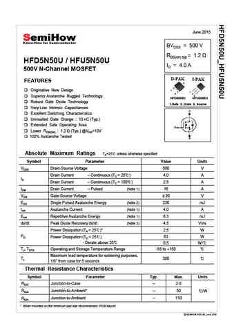
June 2015 BVDSS = 500 V RDS(on) typ HFD5N50U / HFU5N50U ID = 4.0 A 500V N-Channel MOSFET D-PAK I-PAK FEATURES 2 1 Originative New Design 1 3 2 3 Superior Avalanche Rugged Technology HFD5N50U HFU5N50U Robust Gate Oxide Technology 1.Gate 2. Drain 3. Source Very Low Intrinsic Capacitances Excellent Switching Characteristics Unrivalled Gate Charge 13 nC ... See More ⇒
wvm15n50.pdf
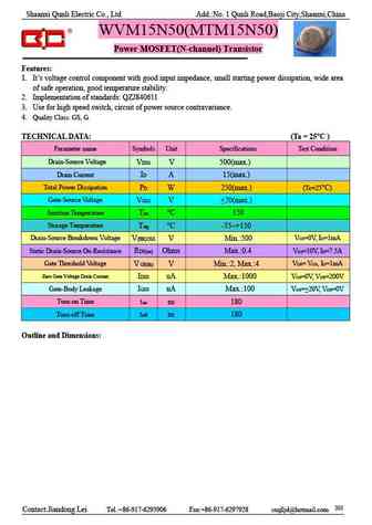
Shaanxi Qunli Electric Co., Ltd Add. No. 1 Qunli Road,Baoji City,Shaanxi,China WVM15N50(MTM15N50) Power MOSFET(N-channel) Transistor Features 1. It s voltage control component with good input impedance, small starting power dissipation, wide area of safe operation, good temperature stability. 2. Implementation of standards QZJ840611 3. Use for high speed switch, circuit of powe... See More ⇒
sl5n50d.pdf
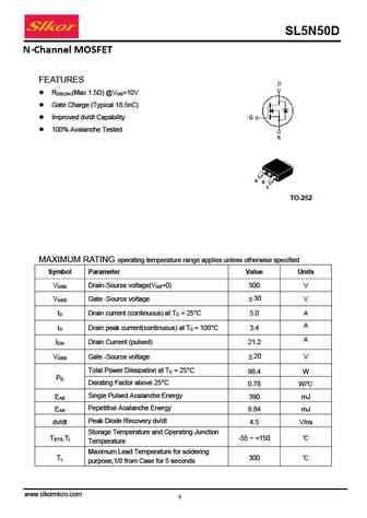
SL5N50D N-Channel MOSFET FEATURES R (Max 1.5 ) @V =10V DS(ON) GS Gate Charge (Typical 18.5nC) Improved dv/dt Capability 100% Avalanche Tested TO-252 MAXIMUM RATING operating temperature range applies unless otherwise specified Symbol Parameter Value Units V Drain-Source voltage(V =0) 500 V DSS GS V Gate -Source voltage 30 V GSS I Drain current (conti... See More ⇒
msu4d5n50q.pdf
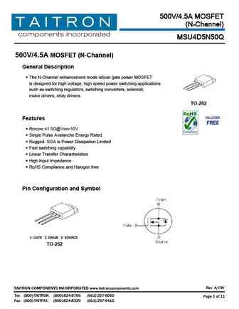
500V/4.5A MOSFET (N-Channel) MSU4D5N50Q 500V/4.5A MOSFET (N-Channel) General Description The N-Channel enhancement mode silicon gate power MOSFET is designed for high voltage, high speed power switching applications such as switching regulators, switching converters, solenoid, motor drivers, relay drivers. TO-262 Features RDS(ON) 1.5 @VGS=10V Single Pul... See More ⇒
p5n50c.pdf
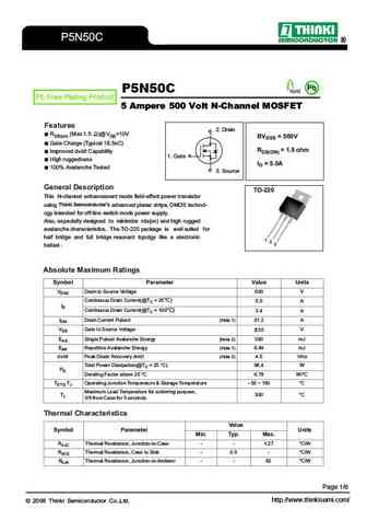
P5N50C Pb P5N50C Pb Free Plating Product 5 Ampere 500 Volt N-Channel MOSFET Features 2. Drain RDS(on) (Max 1.5 )@VGS=10V BVDSS = 500V Gate Charge (Typical 18.5nC) RDS(ON) = 1.5 ohm Improved dv/dt Capability 1. Gate High ruggedness ID = 5.0A 100% Avalanche Tested 3. Source General Description TO-220 This N-channel en... See More ⇒
tmd5n50 tmd5n50g tmu5n50 tmu5n50g.pdf
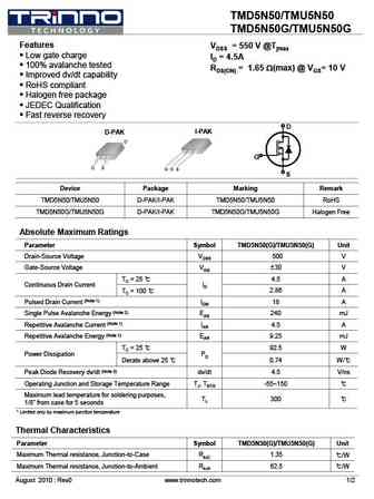
TMD5N50/TMU5N50 TMD5N50G/TMU5N50G Features VDSS = 550 V @Tjmax Low gate charge ID = 4.5A 100% avalanche tested RDS(ON) = 1.65 W(max) @ VGS= 10 V Improved dv/dt capability RoHS compliant Halogen free package JEDEC Qualification Fast reverse recovery D I-PAK D-PAK G S Device Package Marking Remark TMD5N50/TMU5N50 D-PAK/I-PAK TMD5N50/TMU5N50 RoHS ... See More ⇒
tmp5n50sg tmpf5n50sg.pdf
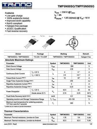
TMP5N50SG/TMPF5N50SG VDSS = 550 V @Tjmax Features ID = 4A Low gate charge RDS(ON) = 1.85 W(max) @ VGS= 10 V 100% avalanche tested Improved dv/dt capability RoHS compliant Halogen free package JEDEC Qualification Fast reverse recovery D G S Device Package Marking Remark TMP5N50SG / TMPF5N50SG TO-220 / TO-220F TMP5N50SG / TMPF5N50SG Halogen Free Abs... See More ⇒
tman15n50.pdf
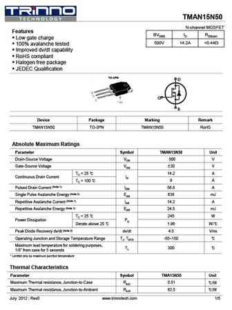
TMAN15N50 N-channel MOSFET Features BVDSS ID RDS(on) Low gate charge 500V 14.2A ... See More ⇒
tmp15n50 tmpf15n50.pdf
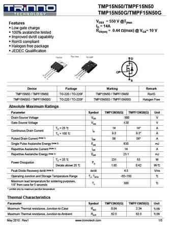
TMP15N50/TMPF15N50 TMP15N50G/TMPF15N50G VDSS = 550 V @Tjmax Features ID = 14A Low gate charge RDS(on) = 0.44 W(max) @ VGS= 10 V 100% avalanche tested Improved dv/dt capability RoHS compliant Halogen free package JEDEC Qualification D G S Device Package Marking Remark TMP15N50 / TMPF15N50 TO-220 / TO-220F TMP15N50 / TMPF15N50 RoHS TMP15N50G / TMPF15N50G... See More ⇒
tmp5n50 tmpf5n50.pdf
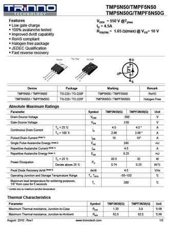
TMP5N50/TMPF5N50 TMP5N50G/TMPF5N50G Features VDSS = 550 V @Tjmax Low gate charge ID = 4.5A 100% avalanche tested RDS(ON) = 1.65 W(max) @ VGS= 10 V Improved dv/dt capability RoHS compliant Halogen free package JEDEC Qualification Fast reverse recovery D G S Device Package Marking Remark TMP5N50 / TMPF5N50 TO-220 / TO-220F TMP5N50 / TMPF5N50 RoHS T... See More ⇒
tsd5n50mr.pdf
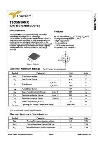
TSD5N50MR 500V N-Channel MOSFET General Description Features This Power MOSFET is produced using Truesemi s 4.5A,500V,Max.RDS(on)=1.6 @ VGS =10V advanced planar stripe DMOS technology. This advanced technology has been especially tailored to Low gate charge(typical 12nC) minimize on-state resistance, provide superior switching High ruggedness performance, an... See More ⇒
wml25n50c4 wmo25n50c4 wmk25n50c4 wmn25n50c4 wmm25n50c4 wmj25n50c4.pdf
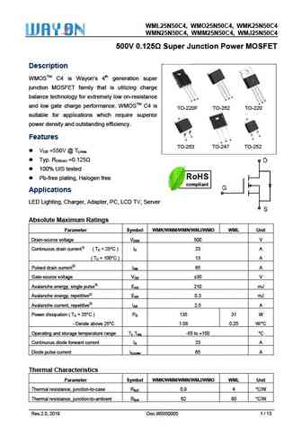
WML25N50C4, WMO25N5 WM C4 W 50C4, MK25N50C WMN2 MJ25N50C 25N50C4, WMM25N50C4, WM C4 500V 0.125 S 0 Super Junction Power MOSFET Descrip ption WMOSTM C4 is Wa 4th generation super ayon s n junction MOSFET fa that is utilizing charge M amily S balance te or extremely esistance echnology fo y low on-re S D D G G G S D G and low ga charge performanc WMOSTM ... See More ⇒
wmo5n50d1b.pdf
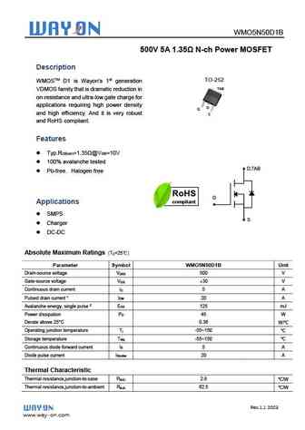
WMO5N50D1B 500V 5A 1.35 N-ch Power MOSFET Description TO-252 WMOSTM D1 is Wayon s 1st generation TAB VDMOS family that is dramatic reduction in on-resistance and ultra-low gate charge for applications requiring high power density D G and high efficiency. And it is very robust S and RoHS compliant. Features Typ.R =1.35 @V =10V DS(on) GS 100% avalan... See More ⇒
wmk15n50d1b wml15n50d1b.pdf
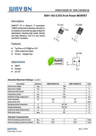
WMK15N50D1B WML15N50D1B 500V 15A 0.37 N-ch Power MOSFET Description TO-220 TO-220F WMOSTM D1 is Wayon s 1st generation VDMOS family that is dramatic reduction in TAB on-resistance and ultra-low gate charge for applications requiring high power density and high efficiency. And it is very robust and RoHS compliant. G G D D S S Features Typ.R =0.37 @V... See More ⇒
cs15n50fa9r.pdf
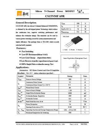
Silicon N-Channel Power MOSFET R CS15N50F A9R General Description VDSS 500 V CS15N50F A9R, the silicon N-channel Enhanced VDMOSFETs, ID 15 A PD(TC=25 ) 70 W is obtained by the self-aligned planar Technology which reduce RDS(ON)Typ 0.3 the conduction loss, improve switching performance and enhance the avalanche energy. The transistor can be used in various ... See More ⇒


fmd5n50e5.pdf
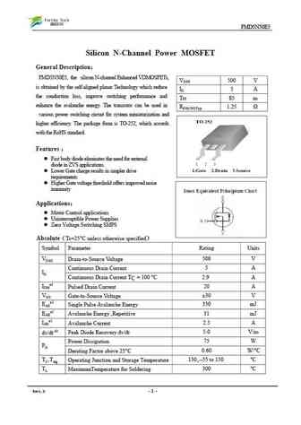
FMD5N50E5 Silicon N-Channel Power MOSFET General Description FMD5N50E5, the silicon N-channel Enhanced VDMOSFETs, VDSS 500 V is obtained by the self-aligned planar Technology which reduce ID 5 A the conduction loss, improve switching performance and Trr 85 ns enhance the avalanche energy. The transistor can be used in RDS(ON)Typ 1.25 various power switching circuit ... See More ⇒
cs15n50f cs15n50p.pdf
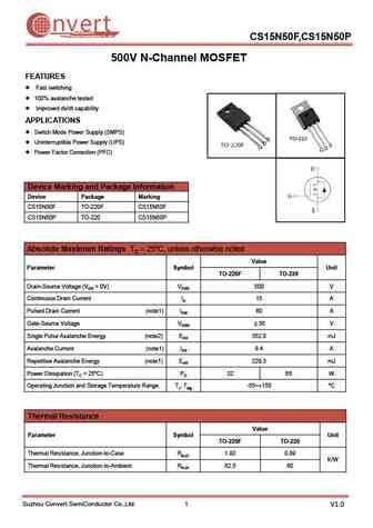
nvert Suzhou Convert Semiconductor Co ., Ltd. CS15N50F,CS15N50P 500V N-Channel MOSFET FEATURES Fast switching 100% avalanche tested Improved dv/dt capability APPLICATIONS Switch Mode Power Supply (SMPS) Uninterruptible Power Supply (UPS) Power Factor Correction (PFC) Device Marking and Package Information Device Package Marking CS15N50F TO-220F CS15N50F CS... See More ⇒
fir5n50fg.pdf
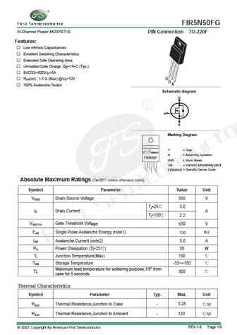
FIR5N50FG N-Channel Power MOSFET-G PIN Connection TO-220F Features Low Intrinsic Capacitances. Excellent Switching Characteristics. Extended Safe Operating Area. Unrivalled Gate Charge Qg=14nC (Typ.). BVDSS=500V,ID=5A RDS(on) 1.5 (Max) @VG=10V G DS 100% Avalanche Tested g Schematic dia ram D G S Marking Diagram Y = Year YAWWVA A = Assembl... See More ⇒
damh75n500h.pdf
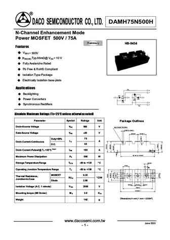
DAMH75N500H DACO SEMICONDUCTOR CO., LTD. N-Channel Enhancement Mode Power MOSFET 500V / 75A Preliminary HB-9434 Features VDSS = 500V RDS(ON) Typ.65 GS Fully Avalanche Rated Pb Free & RoHS Compliant Isolation Type Package Electrically Isolation base plate Applications Backlighting Power Converters Synchronous Rectifiers Absolute Maxim... See More ⇒
hf25n50 hp25n50.pdf
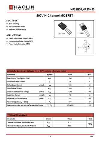
HF25N50,HP25N50 500V N-Channel MOSFET FEATURES Fast switching 100% avalanche tested Improved dv/dt capability APPLICATIONS Switch Mode Power Supply (SMPS) Uninterruptible Power Supply (UPS) Power Factor Correction (PFC) Absolute Maximum Ratings TC = 25 unless otherwise noted C, Parameter Symbol Value Unit Drain-Source Voltage (VGS = 0V) VDSS 500 V Continu... See More ⇒
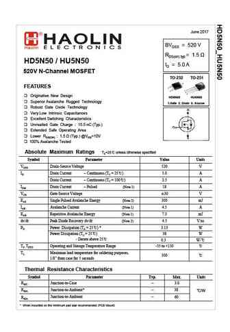
ha25n50.pdf
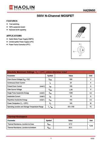
HA25N50 500V N-Channel MOSFET FEATURES Fast switching 100% avalanche tested Improved dv/dt capability APPLICATIONS Switch Mode Power Supply (SMPS) Uninterruptible Power Supply (UPS) Power Factor Correction (PFC) Absolute Maximum Ratings TC = 25 unless otherwise noted C, Parameter Symbol Value Unit Drain-Source Voltage (VGS = 0V) VDSS 500 V Continuous Drai... See More ⇒
jmpc15n50bj.pdf
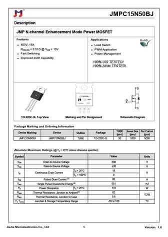
JMPC15N50BJ Description JMP N-channel Enhancement Mode Power MOSFET Features Applications 500V, 15A Load Switch RDS(ON) ... See More ⇒
jmpk5n50bj.pdf
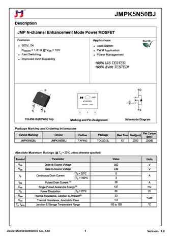
JMPK5N50BJ Description JMP N-channel Enhancement Mode Power MOSFET Features Applications 500V, 5A Load Switch RDS(ON) ... See More ⇒
jmpc25n50bj.pdf
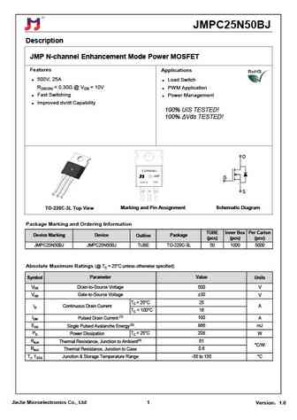
JMPC25N50BJ Description JMP N-channel Enhancement Mode Power MOSFET Features Applications 500V, 25A Load Switch RDS(ON) ... See More ⇒
jmpc5n50bj.pdf

JMPC5N50BJ Description JMP N-channel Enhancement Mode Power MOSFET Features Applications 500V, 5A Load Switch RDS(ON) ... See More ⇒
jmpf5n50bj.pdf

JMPF5N50BJ Description JMP N-channel Enhancement Mode Power MOSFET Features Applications 500V, 5A Load Switch RDS(ON) ... See More ⇒
jmpf15n50bj.pdf
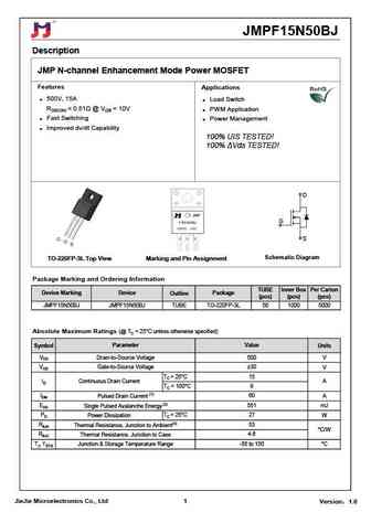
JMPF15N50BJ Description JMP N-channel Enhancement Mode Power MOSFET Features Applications 500V, 15A Load Switch RDS(ON) ... See More ⇒
jmpf25n50bj.pdf
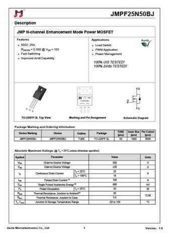
JMPF25N50BJ Description JMP N-channel Enhancement Mode Power MOSFET Features Applications 500V, 25A Load Switch RDS(ON) ... See More ⇒
lnc5n50 lnd5n50 lng5n50 lnh5n50.pdf
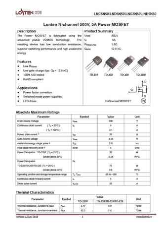
LNC5N50 LND5N50 LNG5N50 LNH5N50 Lonten N-channel 500V, 5A Power MOSFET Description Product Summary The Power MOSFET is fabricated using the V 500V DSS advanced planar VDMOS technology. The I 5A D resulting device has low conduction resistance, R 1.6 DS(on),max superior switching performance and high avalanche Q 12.8 nC g,typ energy. Features Low R DS(on) Low gate charge... See More ⇒
agms5n50d.pdf
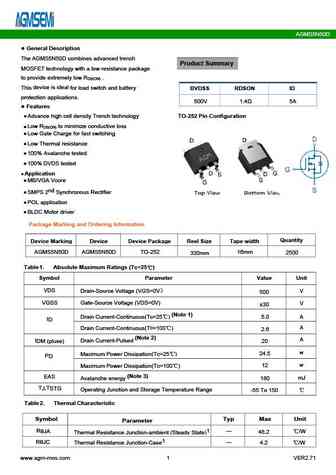
AGMS5N50D General Description The AGMS5N50D combines advanced trench Product Summary MOSFET technology with a low resistance package to provide extremely low R . DS(ON) device is ideal This for load switch and battery BVDSS RDSON ID protection applications. 500V 1.4 5A Features Advance high cell density Trench technology TO-252 Pin Configuration Low R to minimiz... See More ⇒
spd5n50g.pdf
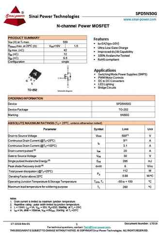
SPD5N50G Sinai Power Technologies www.sinai-power.com N-channel Power MOSFET PRODUCT SUMMARY Features V (V) at T max. 550 DS J ID=5A(Vgs=10V) R max. at 25oC ( ) V =10V 1.5 DS(on) GS Ultra Low Gate Charge Q max. (nC) 42 g Improved dv/dt Capability Q (nC) 12 gs 100% Avalanche Tested Q (nC) 6.5 gd RoHS compliant Configuration single Ap... See More ⇒
se15n50fra.pdf
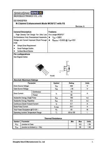
SE15N50FRA N-Channel Enhancement-Mode MOSFET with FR Revision A General Description Features Thigh Density Cell Design For Ultra Low For a single MOSFET On-Resistance Fully Characterized Avalanche VDS = 500V Voltage and Current Improved Shoot-Through RDS(ON) = 0.43 @ VGS=10V FOM Simple Drive Requirement Small Package Outline Surface Mount Device ... See More ⇒
hm25n50.pdf
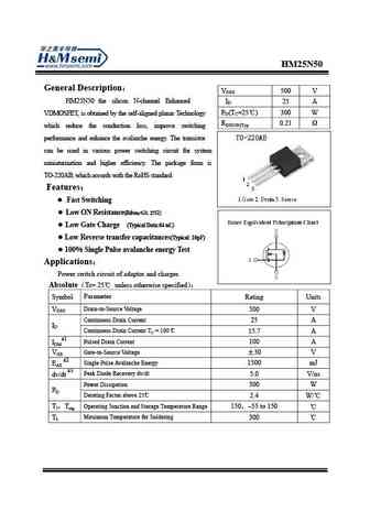
HM25N50 General Description VDSS 500 V HM25N50 the silicon N-channel Enhanced ID 25 A PD(TC=25 ) 300 W VDMOSFET, is obtained by the self-aligned planar Technology RDS(ON)Typ 0.21 which reduce the conduction loss, improve switching performance and enhance the avalanche energy. The transistor can be used in various power switching circuit for system miniaturization a... See More ⇒
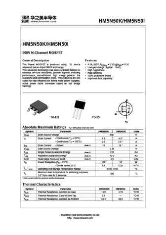
hm15n50 hm15n50f.pdf
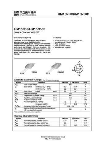
HM15N50/HM15N50F HM15N50/HM15N50F 500V N-Channel MOSFET General Description Features This Power MOSFET is produced using SL semi s 15.0A, 500V, RDS(on) = 0.42 @VGS = 10 V advanced planar stripe DMOS technology. Low gate charge ( typical 45nC) This advanced technology has been espe cially tailored to Fast s witching minimize o n-state r esistance, pr ovide superior switc... See More ⇒
md25n50.pdf
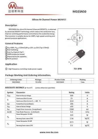
Silicon N-Channel Power MOSFET Description MD25N50 the silicon N-channel Enhanced MOSFETs, is obtained by advanced MOSFET technology which reduce the conduction loss, improve switching performance and enhance the avalanche energy. The transistor is suitable device for SMPS, high speed switching and general purpose applications. General Features V =500V, R ... See More ⇒
mp5n50.pdf
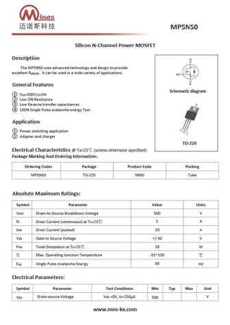
Silicon N-Channel Power MOSFET Description The MP5N50 uses advanced technology and design to provide excellent R . It can be used in a wide variety of applications. DS(ON) General Features Schematic diagram V =500V,I =5A DS D Low ON Resistance Low Reverse transfer capacitances 100% Single Pulse avalanche energy Test Application Power switching application A... See More ⇒
fxn15n50f.pdf
FuXin Semiconductor Co., Ltd. FXN15N50F Series Rev.A General Description Features The FXN15N50F uses advanced Silicon s MOSFET Technology, which V = 500V DS provides high performance in on-state resistance, fast switching ID = 15A @V = 10V GS performance, and excellent quality. Very low on-resistance These devices can also be utilized in industrial a... See More ⇒
fxn25n50f.pdf
FuXin Semiconductor Co., Ltd. FXN25N50F Series Rev.A General Description Features The FXN25N50F uses advanced Silicon s MOSFET Technology, which V = 500V DS provides high performance in on-state resistance, fast switching ID =25A @V = 10V GS performance, and excellent quality. Very low on-resistance These devices can also be utilized in industrial ap... See More ⇒
mpvu5n50ccfd mpvd5n50ccfd.pdf
MPVX5N50CCFD Series Power MOSFET MPSW60M041 FEATURES APPLICATIONS BVDSS 500V, ID=5A Power switch circuit of adaptor and charger RDS(on) 1.7 (Max) @VGS=10V Very Low FOM (RDS(on) *Qg) Excellent stability and uniformity D G TO-252 TO-251 S Ordering Information Type NO. Marking Package Code MPVU5N50CCFD MPVU5N50CCFD TO-251 MPVD5N50CCFD MPVD5N50CCFD TO-252 Abso... See More ⇒
5n50-252.pdf
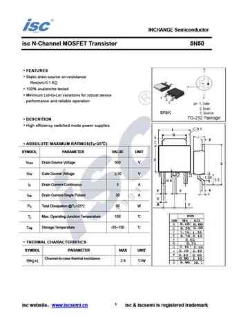
INCHANGE Semiconductor isc N-Channel MOSFET Transistor 5N50 FEATURES Static drain-source on-resistance RDS(on) 1.6 100% avalanche tested Minimum Lot-to-Lot variations for robust device performance and reliable operation DESCRITION High efficiency switched mode power supplies ABSOLUTE MAXIMUM RATINGS(T =25 ) a SYMBOL PARAMETER VALUE UNIT V Drain-Source Voltage ... See More ⇒
aotf5n50.pdf
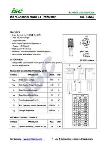
isc N-Channel MOSFET Transistor AOTF5N50 FEATURES Drain Current I = 5.0A@ T =25 D C Drain Source Voltage- V =500V(Min) DSS Static Drain-Source On-Resistance R =1.5 (Max) DS(on) 100% avalanche tested Minimum Lot-to-Lot variations for robust device performance and reliable operation DESCRIPTION Designed for use in switch mode power supplies and general purpos... See More ⇒
mdp5n50bth.pdf
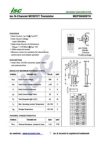
isc N-Channel MOSFET Transistor MDP5N50BTH FEATURES Drain Current I = 5A@ T =25 D C Drain Source Voltage V = 500V(Min) DSS Static Drain-Source On-Resistance R = 1.4 (Max) @V = 10V DS(on) GS 100% avalanche tested Minimum Lot-to-Lot variations for robust device performance and reliable operation DESCRIPTION motor drive, DC-DC converter, power switch and soleno... See More ⇒
fdh15n50.pdf
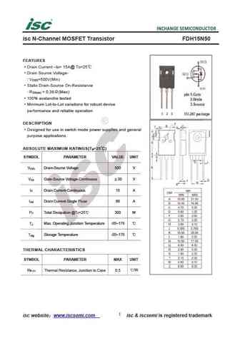
isc N-Channel MOSFET Transistor FDH15N50 FEATURES Drain Current I = 15A@ T =25 D C Drain Source Voltage- V =500V(Min) DSS Static Drain-Source On-Resistance R = 0.38 (Max) DS(on) 100% avalanche tested Minimum Lot-to-Lot variations for robust device performance and reliable operation DESCRIPTION Designed for use in switch mode power supplies and general purpo... See More ⇒
aot5n50.pdf
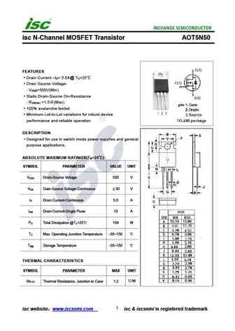
isc N-Channel MOSFET Transistor AOT5N50 FEATURES Drain Current I = 5.0A@ T =25 D C Drain Source Voltage- V =500V(Min) DSS Static Drain-Source On-Resistance R =1.5 (Max) DS(on) 100% avalanche tested Minimum Lot-to-Lot variations for robust device performance and reliable operation DESCRIPTION Designed for use in switch mode power supplies and general purpose... See More ⇒
fdh45n50f.pdf
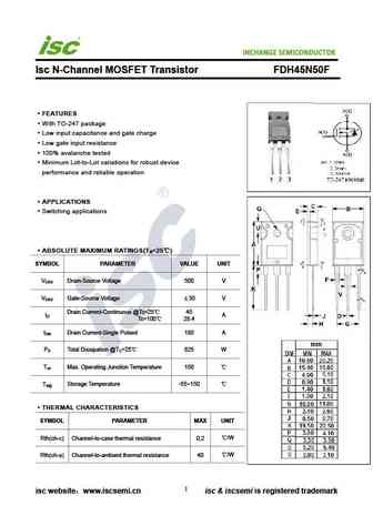
INCHANGE Semiconductor Isc N-Channel MOSFET Transistor FDH45N50F FEATURES With TO-247 package Low input capacitance and gate charge Low gate input resistance 100% avalanche tested Minimum Lot-to-Lot variations for robust device performance and reliable operation APPLICATIONS Switching applications ABSOLUTE MAXIMUM RATINGS(T =25 ) a SYMBOL PARAMETER VALUE UNIT V... See More ⇒
aotf5n50fd.pdf
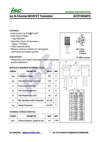
isc N-Channel MOSFET Transistor AOTF5N50FD FEATURES Drain Current I = 5.0A@ T =25 D C Drain Source Voltage- V =500V(Min) DSS Static Drain-Source On-Resistance R =1.8 (Max) DS(on) 100% avalanche tested Minimum Lot-to-Lot variations for robust device performance and reliable operation DESCRIPTION Designed for use in switch mode power supplies and general purp... See More ⇒
mdis5n50th.pdf
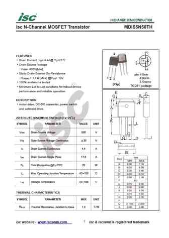
isc N-Channel MOSFET Transistor MDIS5N50TH FEATURES Drain Current I = 4.4A@ T =25 D C Drain Source Voltage V = 400V(Min) DSS Static Drain-Source On-Resistance R = 1.4 (Max) @V = 10V DS(on) GS 100% avalanche tested Minimum Lot-to-Lot variations for robust device performance and reliable operation DESCRIPTION motor drive, DC-DC converter, power switch and sole... See More ⇒
aod5n50.pdf
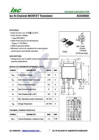
isc N-Channel MOSFET Transistor AOD5N50 FEATURES Drain Current I = 5.0A@ T =25 D C Drain Source Voltage- V =500V(Min) DSS Static Drain-Source On-Resistance R =1.6 (Max) DS(on) 100% avalanche tested Minimum Lot-to-Lot variations for robust device performance and reliable operation DESCRIPTION Designed for use in switch mode power supplies and general purpose... See More ⇒
mdp5n50th.pdf
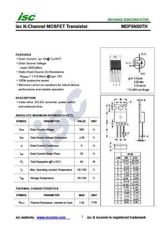
isc N-Channel MOSFET Transistor MDP5N50TH FEATURES Drain Current I = 5A@ T =25 D C Drain Source Voltage V = 500V(Min) DSS Static Drain-Source On-Resistance R = 1.4 (Max) @V = 10V DS(on) GS 100% avalanche tested Minimum Lot-to-Lot variations for robust device performance and reliable operation DESCRIPTION motor drive, DC-DC converter, power switch and solenoi... See More ⇒
ap5n50d.pdf
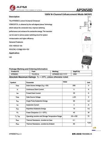
AP5N50D 500V N-Channel Enhancement Mode MOSFE Description The AP5N50D is silicon N-channel Enhanced VDMOSFETs, is obtained by the self-aligned planar Technology which reduce the conduction loss, improve switching performance and enhance the avalanche energy. The transistor can be used in various power switching circuit for system miniaturization and higher efficiency. General... See More ⇒
ap5n50f ap5n50p ap5n50t.pdf
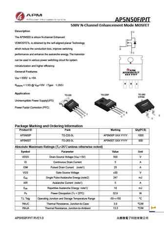
AP5N50FIPIT 500V N-Channel Enhancement Mode MOSFET Description The AP5N50D is silicon N-channel Enhanced VDMOSFETs, is obtained by the self-aligned planar Technology which reduce the conduction loss, improve switching performance and enhance the avalanche energy. The transistor can be used in various power switching circuit for system miniaturization and higher efficiency. Ge... See More ⇒
ap5n50bd.pdf
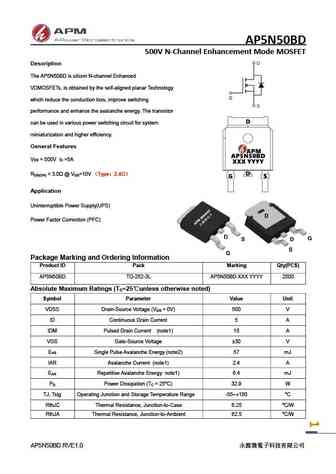
AP5N50BD 500V N-Channel Enhancement Mode MOSFET Description The AP5N50BD is silicon N-channel Enhanced VDMOSFETs, is obtained by the self-aligned planar Technology which reduce the conduction loss, improve switching performance and enhance the avalanche energy. The transistor can be used in various power switching circuit for system miniaturization and higher efficiency. Gene... See More ⇒
Detailed specifications: UF450, UF460, 1N50, 1N50Z, 2N50, 3N50, 3N50Z, 4N50, AO3401, 5N50K, 6N50, 7N50, 8N50, 1N40, 2N40, 3N40, 4N40
Keywords - 5N50 MOSFET specs
5N50 cross reference
5N50 equivalent finder
5N50 pdf lookup
5N50 substitution
5N50 replacement
Step-by-step guide to finding a MOSFET replacement. Cross-reference parts and ensure compatibility for your repair or project.
MOSFET Parameters. How They Affect Each Other
🌐 : EN ES РУ

LIST
Last Update
MOSFET: CEZC2P07 | CEZ2R05 | CEU3133 | CES2361 | CES2312A | CEP100N10L | CEM3425 | CEM3139 | CEM3133 | CEM3115
Popular searches
2sc2362 | 2sd468 | c2240 transistor | 2sc1918 | c1213 transistor | 2sc1400 replacement | 2sb817 | mn2488 datasheet