12N30 Datasheet. Specs and Replacement
Type Designator: 12N30 📄📄
Type of Transistor: MOSFET
Type of Control Channel: N-Channel
Absolute Maximum Ratings
Pd ⓘ - Maximum Power Dissipation: 83 W
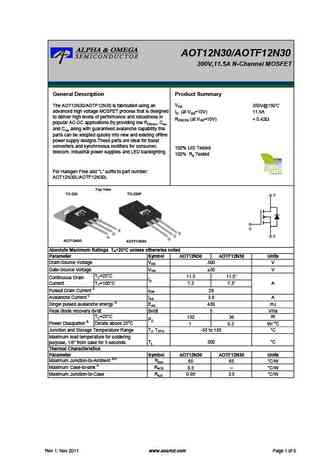
|Vds|ⓘ - Maximum Drain-Source Voltage: 300 V
|Vgs|ⓘ - Maximum Gate-Source Voltage: 20 V
|Id| ⓘ - Maximum Drain Current: 12 A
Tj ⓘ - Maximum Junction Temperature: 150 °C
Electrical Characteristics
tr ⓘ - Rise Time: 105 nS
Cossⓘ - Output Capacitance: 900 pF
RDSonⓘ - Maximum Drain-Source On-State Resistance: 0.34 Ohm
Package: TO-252
📄📄 Copy
- MOSFET ⓘ Cross-Reference Search
12N30 datasheet
..1. Size:158K utc
12n30.pdf 
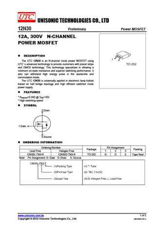
UNISONIC TECHNOLOGIES CO., LTD 12N30 Preliminary Power MOSFET 12A, 300V N-CHANNEL POWER MOSFET DESCRIPTION The UTC 12N30 is an N-channel mode power MOSFET using UTC s advanced technology to provide customers with planar stripe and DMOS technology. This technology specializes in allowing a minimum on-state resistance and superior switching performance. It also can withstand ... See More ⇒
0.1. Size:176K ixys
ixbt12n300.pdf

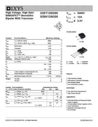
High Voltage, High Gain VCES = 3000V IXBT12N300 BIMOSFETTM Monolithic IXBH12N300 IC110 = 12A Bipolar MOS Transistor VCE(sat) 3.2V TO-268 (IXBT) G Symbol Test Conditions Maximum Ratings E VCES TC = 25 C to 150 C 3000 V C (Tab) VCGR TJ = 25 C to 150 C, RGE = 1M 3000 V VGES Continuous 20 V TO-247 (IXBH) VGEM Transient 30 V IC25 TC = 25 C 30 A ... See More ⇒
0.2. Size:176K ixys
ixbh12n300.pdf
High Voltage, High Gain VCES = 3000V IXBT12N300 BIMOSFETTM Monolithic IXBH12N300 IC110 = 12A Bipolar MOS Transistor VCE(sat) 3.2V TO-268 (IXBT) G Symbol Test Conditions Maximum Ratings E VCES TC = 25 C to 150 C 3000 V C (Tab) VCGR TJ = 25 C to 150 C, RGE = 1M 3000 V VGES Continuous 20 V TO-247 (IXBH) VGEM Transient 30 V IC25 TC = 25 C 30 A ... See More ⇒
0.3. Size:246K ixys
ixbt12n300hv.pdf
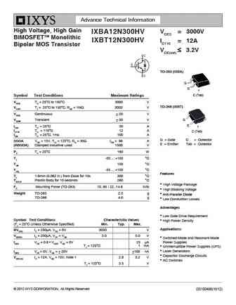
Advance Technical Information High Voltage, High Gain VCES = 3000V IXBA12N300HV BIMOSFETTM Monolithic IXBT12N300HV IC110 = 12A Bipolar MOS Transistor VCE(sat) 3.2V TO-263 (IXBA) G E C (Tab) Symbol Test Conditions Maximum Ratings VCES TC = 25 C to 150 C 3000 V TO-268 (IXBT) VCGR TJ = 25 C to 150 C, RGE = 1M 3000 V VGES Continuous 20 V VGEM Trans... See More ⇒
0.4. Size:195K ixys
ixbf12n300.pdf
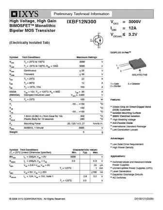
Preliminary Technical Information High Voltage, High Gain VCES = 3000V IXBF12N300 BIMOSFETTM Monolithic IC90 = 12A Bipolar MOS Transistor VCE(sat) 3.2V (Electrically Isolated Tab) ISOPLUS i4-PakTM Symbol Test Conditions Maximum Ratings VCES TC = 25 C to 150 C 3000 V 1 VCGR TJ = 25 C to 150 C, RGE = 1M 3000 V 2 VGES Continuous 20 V 5 VGEM Transie... See More ⇒
0.5. Size:246K ixys
ixba12n300hv.pdf

Advance Technical Information High Voltage, High Gain VCES = 3000V IXBA12N300HV BIMOSFETTM Monolithic IXBT12N300HV IC110 = 12A Bipolar MOS Transistor VCE(sat) 3.2V TO-263 (IXBA) G E C (Tab) Symbol Test Conditions Maximum Ratings VCES TC = 25 C to 150 C 3000 V TO-268 (IXBT) VCGR TJ = 25 C to 150 C, RGE = 1M 3000 V VGES Continuous 20 V VGEM Trans... See More ⇒
0.6. Size:252K ixys
mmix4b12n300.pdf
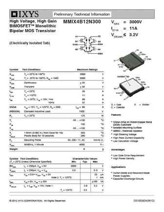
Preliminary Technical Information High Voltage, High Gain MMIX4B12N300 VCES = 3000V BIMOSFETTM Monolithic IC110 = 11A Bipolar MOS Transistor VCE(sat) 3.2V C2 C1 G1 G2 (Electrically Isolated Tab) E2C4 E1C3 G3 G4 C2 G2 E3E4 E2C4 G4 E3E4 C1 G1 E1C3 Symbol Test Conditions Maximum Ratings G3 VCES TC = 25 C to 150 C 3000 V Isolated Tab E3E4 VCG... See More ⇒
0.7. Size:462K kec
kmb012n30q.pdf
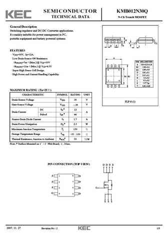
SEMICONDUCTOR KMB012N30Q TECHNICAL DATA N-Ch Trench MOSFET General Description Switching regulator and DC-DC Converter applications. It s mainly suitable for power management in PC, portable equipment and battery powered systems. H T D P G L FEATURES VDSS=30V, ID=12A. A Low Drain-Source ON Resistance. DIM MILLIMETERS RDS(ON)=7m (Max.) @ VGS=10V A 5.05+0.25/-0.20 RDS(ON)=11... See More ⇒
0.8. Size:803K kec
kmb012n30qa.pdf
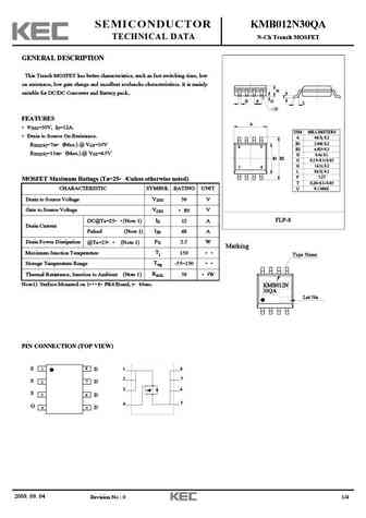
SEMICONDUCTOR KMB012N30QA TECHNICAL DATA N-Ch Trench MOSFET GENERAL DESCRIPTION This Trench MOSFET has better characteristics, such as fast switching time, low on resistance, low gate charge and excellent avalanche characteristiscs. It is mainly H suitable for DC/DC Converter and Battery pack.. T D P G L U FEATURES A VDSS=30V, ID=12A. DIM MILLIMETERS Drain to Source On Resis... See More ⇒
0.9. Size:324K aosemi
aot12n30.pdf
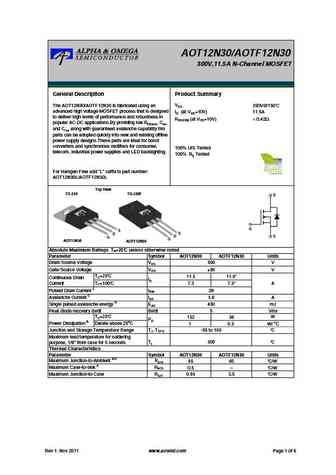
AOT12N30/AOTF12N30 300V,11.5A N-Channel MOSFET General Description Product Summary VDS 350V@150 The AOT12N30/AOTF12N30 is fabricated using an advanced high voltage MOSFET process that is designed ID (at VGS=10V) 11.5A to deliver high levels of performance and robustness in RDS(ON) (at VGS=10V) ... See More ⇒
0.10. Size:324K aosemi
aotf12n30.pdf

AOT12N30/AOTF12N30 300V,11.5A N-Channel MOSFET General Description Product Summary VDS 350V@150 The AOT12N30/AOTF12N30 is fabricated using an advanced high voltage MOSFET process that is designed ID (at VGS=10V) 11.5A to deliver high levels of performance and robustness in RDS(ON) (at VGS=10V) ... See More ⇒
0.11. Size:378K aosemi
aot12n30 aotf12n30.pdf
AOT12N30/AOTF12N30 300V,11.5A N-Channel MOSFET General Description Product Summary VDS 350V@150 The AOT12N30/AOTF12N30 is fabricated using an advanced high voltage MOSFET process that is designed ID (at VGS=10V) 11.5A to deliver high levels of performance and robustness in RDS(ON) (at VGS=10V) ... See More ⇒
0.12. Size:463K cystek
mtn12n30fp.pdf
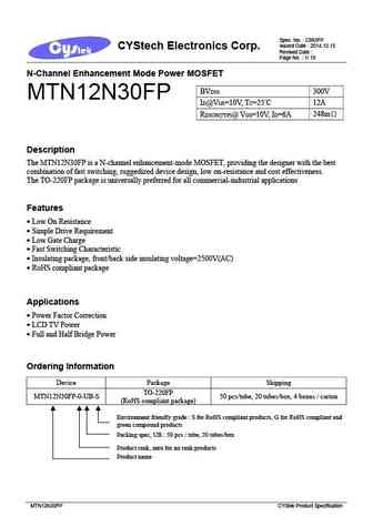
Spec. No. C993FP Issued Date 2014.12.15 CYStech Electronics Corp. Revised Date Page No. 1/ 10 N-Channel Enhancement Mode Power MOSFET BVDSS 300V MTN12N30FP ID@VGS=10V, TC=25 C 12A RDSON(TYP)@ VGS=10V, ID=6A 248m Description The MTN12N30FP is a N-channel enhancement-mode MOSFET, providing the designer with the best combination of fast switching, ruggedized devic... See More ⇒
0.13. Size:261K inchange semiconductor
aot12n30.pdf
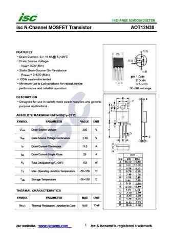
isc N-Channel MOSFET Transistor AOT12N30 FEATURES Drain Current I = 11.5A@ T =25 D C Drain Source Voltage- V = 300V(Min) DSS Static Drain-Source On-Resistance R = 0.42 (Max) DS(on) 100% avalanche tested Minimum Lot-to-Lot variations for robust device performance and reliable operation DESCRIPTION Designed for use in switch mode power supplies and general pu... See More ⇒
0.14. Size:252K inchange semiconductor
aotf12n30.pdf
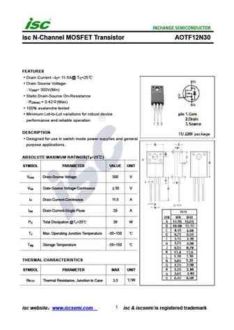
isc N-Channel MOSFET Transistor AOTF12N30 FEATURES Drain Current I = 11.5A@ T =25 D C Drain Source Voltage- V = 300V(Min) DSS Static Drain-Source On-Resistance R = 0.42 (Max) DS(on) 100% avalanche tested Minimum Lot-to-Lot variations for robust device performance and reliable operation DESCRIPTION Designed for use in switch mode power supplies and general p... See More ⇒
Detailed specifications: UF740, UF3N25, UF634, 12N25, 15N25, 18N25, UF2N30, 10N30, K3569, UF3205, 2N7000Z, 2N7002LL, 2N7002Z, 2N7002ZT, UF3055, UTD3055, 12N06
Keywords - 12N30 MOSFET specs
12N30 cross reference
12N30 equivalent finder
12N30 pdf lookup
12N30 substitution
12N30 replacement
Can't find your MOSFET?
Learn how to find a substitute transistor by analyzing voltage, current and package compatibility
