12N10 Datasheet. Specs and Replacement
Type Designator: 12N10 📄📄
Type of Transistor: MOSFET
Type of Control Channel: N-Channel
Absolute Maximum Ratings
Pd ⓘ - Maximum Power Dissipation: 73 W
|Vds|ⓘ - Maximum Drain-Source Voltage: 100 V
|Vgs|ⓘ - Maximum Gate-Source Voltage: 20 V
|Id| ⓘ - Maximum Drain Current: 12 A
Tj ⓘ - Maximum Junction Temperature: 150 °C
Electrical Characteristics
tr ⓘ - Rise Time: 7 nS
Cossⓘ - Output Capacitance: 90 pF
📄📄 Copy
12N10 substitution
- MOSFET ⓘ Cross-Reference Search
12N10 datasheet
12n10.pdf
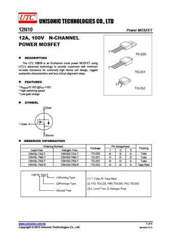
UNISONIC TECHNOLOGIES CO., LTD 12N10 Power MOSFET 12A, 100V N-CHANNEL POWER MOSFET DESCRIPTION The UTC 12N10 is an N-channel mode power MOSFET using UTC s advanced technology to provide customers with minimum on-state resistance for extremely high dense cell design, rugged avalanche characteristics and less critical alignment steps. FEATURES * RDS(on)... See More ⇒
12n10.pdf
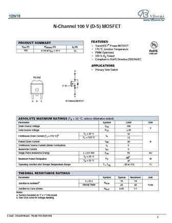
12N10 www.VBsemi.tw N-Channel 100 V (D-S) MOSFET FEATURES PRODUCT SUMMARY TrenchFET Power MOSFET VDS (V) RDS(on) ( )ID (A) 175 C Junction Temperature 100 0.11 4 at VGS = 10 V 15 PWM Optimized 100 % Rg Tested Compliant to RoHS Directive 2002/95/EC APPLICATIONS Primary Side Switch D TO-252 G S G D S N-Channel MOSFET ABSOLUTE MAXIMUM RATINGS (TA... See More ⇒
mtp12n10erev1a.pdf

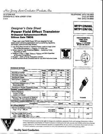
MOTOROLA Order this document SEMICONDUCTOR TECHNICAL DATA by MTP12N10E/D Designer's Data Sheet MTP12N10E TMOS E-FET. Motorola Preferred Device Power Field Effect Transistor N Channel Enhancement Mode Silicon Gate TMOS POWER FET This advanced TMOS E FET is designed to withstand high 12 AMPERES energy in the avalanche and commutation modes. The new energy 100 VOLTS effi... See More ⇒
mtp12n10e.pdf
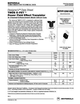
MOTOROLA Order this document SEMICONDUCTOR TECHNICAL DATA by MTP12N10E/D Designer's Data Sheet MTP12N10E TMOS E-FET. Motorola Preferred Device Power Field Effect Transistor N Channel Enhancement Mode Silicon Gate TMOS POWER FET This advanced TMOS E FET is designed to withstand high 12 AMPERES energy in the avalanche and commutation modes. The new energy 100 VOLTS effi... See More ⇒
php12n10e 1.pdf
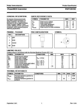
Philips Semiconductors Product Specification PowerMOS transistor PHP12N10E GENERAL DESCRIPTION QUICK REFERENCE DATA N-channel enhancement mode SYMBOL PARAMETER MAX. UNIT field-effect power transistor in a plastic envelope. The device is VDS Drain-source voltage 100 V intended for use in Switched Mode ID Drain current (DC) 14 A Power Supplies (SMPS), motor Ptot Total power dissipation 7... See More ⇒
phd12n10e 2.pdf
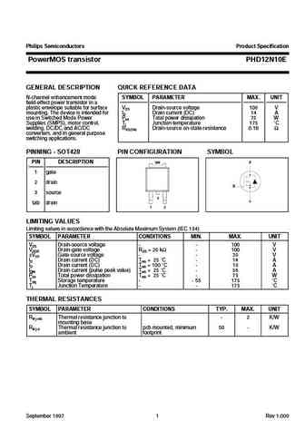
Philips Semiconductors Product Specification PowerMOS transistor PHD12N10E GENERAL DESCRIPTION QUICK REFERENCE DATA N-channel enhancement mode SYMBOL PARAMETER MAX. UNIT field-effect power transistor in a plastic envelope suitable for surface VDS Drain-source voltage 100 V mounting. The device is intended for ID Drain current (DC) 14 A use in Switched Mode Power Ptot Total power dissip... See More ⇒
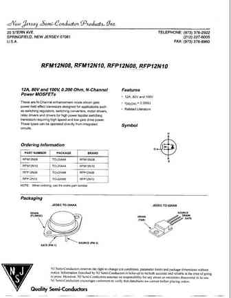
rfp12n10l.pdf
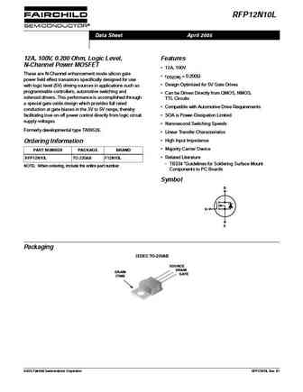
RFP12N10L Data Sheet April 2005 12A, 100V, 0.200 Ohm, Logic Level, Features N-Channel Power MOSFET 12A, 100V These are N-Channel enhancement mode silicon gate rDS(ON) = 0.200 power field effect transistors specifically designed for use Design Optimized for 5V Gate Drives with logic level (5V) driving sources in applications such as programmable controllers, automotiv... See More ⇒
ixgp12n100.pdf

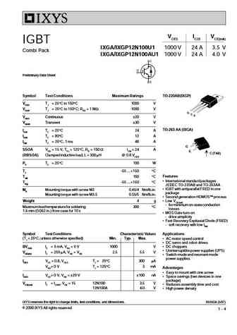
VCES IC25 VCE(sat) IGBT IXGA/IXGP12N100 1000 V 24 A 3.5 V IXGA/IXGP12N100A 1000 V 24 A 4.0 V Preliminary Data Sheet TO-220AB (IXGP) Symbol Test Conditions Maximum Ratings VCES TJ = 25 C to 150 C 1000 V VCGR TJ = 25 C to 150 C; RGE = 1 MW 1000 V G VGES Continuous 20 V C E VGEM Transient 30 V IC25 TC = 25 C24 A TO-263 (IXGA) IC90 TC = 90 C12 A ICM TC = 25 C, 1 ms 48 A ... See More ⇒
ixth10n100 ixtm10n100 ixth12n100 ixtm12n100.pdf
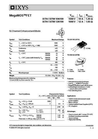
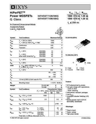
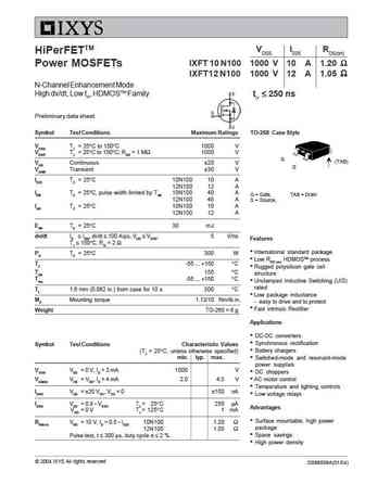
VDSS ID25 RDS(on) MegaMOSTMFET IXTH / IXTM 10N100 1000 V 10 A 1.20 IXTH / IXTM 12N100 1000 V 12 A 1.05 N-Channel Enhancement Mode Symbol Test Conditions Maximum Ratings TO-247 AD (IXTH) VDSS TJ = 25 C to 150 C 1000 V VDGR TJ = 25 C to 150 C; RGS = 1 M 1000 V VGS Continuous 20 V D (TAB) VGSM Transient 30 V ID25 TC = 25 C 10N... See More ⇒
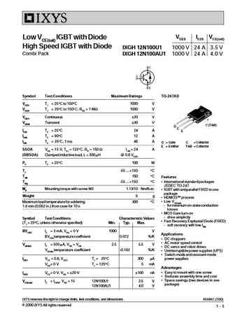
ixgh12n100u1.pdf

VCES IC25 VCE(sat) Low VCE(sat) IGBT with Diode High Speed IGBT with Diode IXGH 12N100U1 1000 V 24 A 3.5 V Combi Pack IXGH 12N100AU1 1000 V 24 A 4.0 V Symbol Test Conditions Maximum Ratings TO-247AD VCES TJ = 25 C to 150 C 1000 V VCGR TJ = 25 C to 150 C; RGE = 1 MW 1000 V VGES Continuous 20 V VGEM Transient 30 V C (TAB) G C IC25 TC = 25 C24 A E IC90 TC = 90 C12 A ICM ... See More ⇒
ixgp12n100a.pdf

VCES IC25 VCE(sat) IGBT IXGA/IXGP12N100 1000 V 24 A 3.5 V IXGA/IXGP12N100A 1000 V 24 A 4.0 V Preliminary Data Sheet TO-220AB (IXGP) Symbol Test Conditions Maximum Ratings VCES TJ = 25 C to 150 C 1000 V VCGR TJ = 25 C to 150 C; RGE = 1 MW 1000 V G VGES Continuous 20 V C E VGEM Transient 30 V IC25 TC = 25 C24 A TO-263 (IXGA) IC90 TC = 90 C12 A ICM TC = 25 C, 1 ms 48 A ... See More ⇒
ixgh12n100au1.pdf
VCES IC25 VCE(sat) Low VCE(sat) IGBT with Diode High Speed IGBT with Diode IXGH 12N100U1 1000 V 24 A 3.5 V Combi Pack IXGH 12N100AU1 1000 V 24 A 4.0 V Symbol Test Conditions Maximum Ratings TO-247AD VCES TJ = 25 C to 150 C 1000 V VCGR TJ = 25 C to 150 C; RGE = 1 MW 1000 V VGES Continuous 20 V VGEM Transient 30 V C (TAB) G C IC25 TC = 25 C24 A E IC90 TC = 90 C12 A ICM ... See More ⇒
ixgp12n100u1.pdf

VCES IC25 VCE(sat) IGBT IXGA/IXGP12N100U1 1000 V 24 A 3.5 V Combi Pack IXGA/IXGP12N100AU1 1000 V 24 A 4.0 V Preliminary Data Sheet Symbol Test Conditions Maximum Ratings TO-220AB(IXGP) VCES TJ = 25 C to 150 C 1000 V VCGR TJ = 25 C to 150 C; RGE = 1 MW 1000 V G C E VGES Continuous 20 V VGEM Transient 30 V TO-263 AA (IXGA) IC25 TC = 25 C24 A IC90 TC = 90 C12 A ICM TC = ... See More ⇒
ixgh12n100.pdf
VCES IC25 VCE(sat) Low VCE(sat) IGBT High Speed IGBT IXGH 12N100 1000 V 24 A 3.5 V IXGH 12N100A 1000 V 24 A 4.0 V Symbol Test Conditions Maximum Ratings TO-247AD VCES TJ = 25 C to 150 C 1000 V VCGR TJ = 25 C to 150 C; RGE = 1 MW 1000 V VGES Continuous 20 V C (TAB) G C VGEM Transient 30 V E IC25 TC = 25 C24 A G = Gate C = Collector IC90 TC = 90 C12 A E = Emitter TAB = ... See More ⇒
ixft12n100qhv.pdf
Advance Technical Information High Voltage HiPerFETTM VDSS = 1000V IXFT12N100QHV Power MOSFET ID25 = 12A Q-CLASS RDS(on) 1.05 N-Channel Enhancement Mode Fast Intrinsic Diode TO-268S G Symbol Test Conditions Maximum Ratings S VDSS TJ = 25 C to 150 C 1000 V D (Tab) VDGR TJ = 25 C to 150 C, RGS = 1M 1000 V VGSS Continuous 20 V G = Ga... See More ⇒
ixga12n100 ixgp12n100 ixga12n100a ixgp12n100a.pdf
VCES IC25 VCE(sat) IGBT IXGA/IXGP12N100 1000 V 24 A 3.5 V IXGA/IXGP12N100A 1000 V 24 A 4.0 V Preliminary Data Sheet TO-220AB (IXGP) Symbol Test Conditions Maximum Ratings VCES TJ = 25 C to 150 C 1000 V VCGR TJ = 25 C to 150 C; RGE = 1 MW 1000 V G VGES Continuous 20 V C E VGEM Transient 30 V IC25 TC = 25 C24 A TO-263 (IXGA) IC90 TC = 90 C12 A ICM TC = 25 C, 1 ms 48 A ... See More ⇒
ixga12n100u1 ixgp12n100u1 ixga12n100au1 ixgp12n100au1.pdf
VCES IC25 VCE(sat) IGBT IXGA/IXGP12N100U1 1000 V 24 A 3.5 V Combi Pack IXGA/IXGP12N100AU1 1000 V 24 A 4.0 V Preliminary Data Sheet Symbol Test Conditions Maximum Ratings TO-220AB(IXGP) VCES TJ = 25 C to 150 C 1000 V VCGR TJ = 25 C to 150 C; RGE = 1 MW 1000 V G C E VGES Continuous 20 V VGEM Transient 30 V TO-263 AA (IXGA) IC25 TC = 25 C24 A IC90 TC = 90 C12 A ICM TC = ... See More ⇒
ixft12n100q ixfh12n100q ixft10n100q ixfh10n100q.pdf
VDSS ID25 RDS(on) HiPerFETTM IXFH/IXFT12N100Q 1000 V 12 A 1.05 Power MOSFETs IXFH/IXFT10N100Q 1000 V 10 A 1.20 Q Class trr 250 ns N-Channel Enhancement Mode Avalanche Rated Low Qg, High dv/dt Symbol Test Conditions Maximum Ratings TO-247 AD (IXFH) VDSS TJ = 25 C to 150 C 1000 V VDGR TJ = 25 C to 150 C; RGS... See More ⇒
ixgh12n100a.pdf

VCES IC25 VCE(sat) Low VCE(sat) IGBT High Speed IGBT IXGH 12N100 1000 V 24 A 3.5 V IXGH 12N100A 1000 V 24 A 4.0 V Symbol Test Conditions Maximum Ratings TO-247AD VCES TJ = 25 C to 150 C 1000 V VCGR TJ = 25 C to 150 C; RGE = 1 MW 1000 V VGES Continuous 20 V C (TAB) G C VGEM Transient 30 V E IC25 TC = 25 C24 A G = Gate C = Collector IC90 TC = 90 C12 A E = Emitter TAB = ... See More ⇒
ixfr10n100f ixfr12n100f.pdf
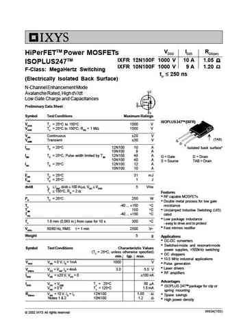
VDSS ID25 RDS(on) HiPerFETTM Power MOSFETs IXFR 12N100F 1000 V 10 A 1.05 ISOPLUS247TM IXFR 10N100F 1000 V 9 A 1.20 F-Class MegaHertz Switching trr 250 ns (Electrically Isolated Back Surface) N-Channel Enhancement Mode Avalanche Rated, High dV/dt Low Gate Charge and Capacitances Preliminary Data Sheet Symbol ... See More ⇒
ixz4df12n100.pdf
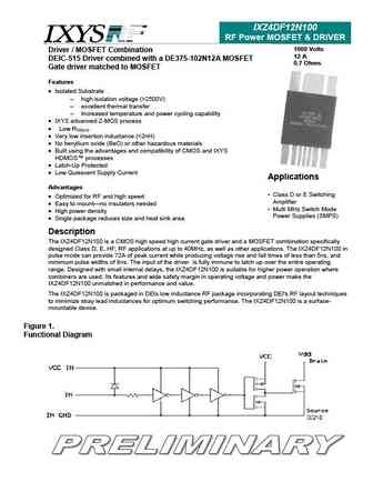
IXZ4DF12N100 RF Power MOSFET & DRIVER 1000 Volts Driver / MOSFET Combination 12 A DEIC-515 Driver combined with a DE375-102N12A MOSFET 0.7 Ohms Gate driver matched to MOSFET Features Isolated Substrate - high isolation voltage (>2500V) - excellent thermal transfer - Increased temperature and power cycling capability IXYS advanced Z-MOS process Low RDS(on)... See More ⇒
ixgp12n100au1.pdf

VCES IC25 VCE(sat) IGBT IXGA/IXGP12N100U1 1000 V 24 A 3.5 V Combi Pack IXGA/IXGP12N100AU1 1000 V 24 A 4.0 V Preliminary Data Sheet Symbol Test Conditions Maximum Ratings TO-220AB(IXGP) VCES TJ = 25 C to 150 C 1000 V VCGR TJ = 25 C to 150 C; RGE = 1 MW 1000 V G C E VGES Continuous 20 V VGEM Transient 30 V TO-263 AA (IXGA) IC25 TC = 25 C24 A IC90 TC = 90 C12 A ICM TC = ... See More ⇒
ixfr10n100q ixfr12n100q.pdf
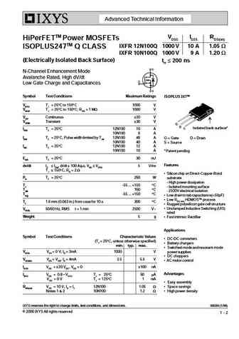
Advanced Technical Information VDSS ID25 RDS(on) HiPerFETTM Power MOSFETs IXFR 12N100Q 1000 V 10 A 1.05 W ISOPLUS247TM Q CLASS IXFR 10N100Q 1000 V 9 A 1.20 W (Electrically Isolated Back Surface) trr 200 ns N-Channel Enhancement Mode Avalanche Rated, High dV/dt Low Gate Charge and Capacitances Symbol Test Conditions Maximum Ratings ISOPLUS 247TM VDSS TJ = 25 C to 150 C 1000 V ... See More ⇒
ixgh12n100 ixgh12n100a.pdf

VCES IC25 VCE(sat) Low VCE(sat) IGBT High Speed IGBT IXGH 12N100 1000 V 24 A 3.5 V IXGH 12N100A 1000 V 24 A 4.0 V Symbol Test Conditions Maximum Ratings TO-247AD VCES TJ = 25 C to 150 C 1000 V VCGR TJ = 25 C to 150 C; RGE = 1 MW 1000 V VGES Continuous 20 V C (TAB) G C VGEM Transient 30 V E IC25 TC = 25 C24 A G = Gate C = Collector IC90 TC = 90 C12 A E = Emitter TAB = ... See More ⇒
rfp12n10l.pdf

Is Now Part of To learn more about ON Semiconductor, please visit our website at www.onsemi.com Please note As part of the Fairchild Semiconductor integration, some of the Fairchild orderable part numbers will need to change in order to meet ON Semiconductor s system requirements. Since the ON Semiconductor product management systems do not have the ability to manage part nomenclatur... See More ⇒
ntd12n10g ntd12n10t4.pdf
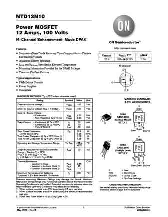
NTD12N10 Power MOSFET 12 Amps, 100 Volts N-Channel Enhancement-Mode DPAK http //onsemi.com Features Source-to-Drain Diode Recovery Time Comparable to a Discrete V(BR)DSS RDS(on) TYP ID MAX Fast Recovery Diode 100 V 165 mW @ 10 V 12 A Avalanche Energy Specified IDSS and RDS(on) Specified at Elevated Temperature N-Channel Mounting Information Provided for the DPAK Pac... See More ⇒
ntd12n10.pdf

NTD12N10 Power MOSFET 12 Amps, 100 Volts N-Channel Enhancement-Mode DPAK http //onsemi.com Features Source-to-Drain Diode Recovery Time Comparable to a Discrete V(BR)DSS RDS(on) TYP ID MAX Fast Recovery Diode 100 V 165 mW @ 10 V 12 A Avalanche Energy Specified IDSS and RDS(on) Specified at Elevated Temperature N-Channel Mounting Information Provided for the DPAK Pac... See More ⇒
12n10l-ta3-t 12n10g-ta3-t 12n10l-tm3-t 12n10g-tm3-t 12n10l-tn3-r 12n10g-tn3-r 12n10g-s08-r.pdf
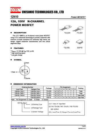
UNISONIC TECHNOLOGIES CO., LTD 12N10 Power MOSFET 12A, 100V N-CHANNEL POWER MOSFET DESCRIPTION The UTC 12N10 is an N-channel mode power MOSFET using UTC s advanced technology to provide customers with minimum on-state resistance for extremely high dense cell design, rugged avalanche characteristics and less critical alignment steps. FEATURES * RDS(on) ... See More ⇒
ut12n10.pdf
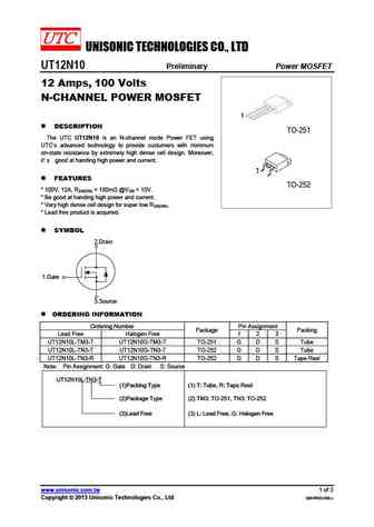
UNISONIC TECHNOLOGIES CO., LTD UT12N10 Preliminary Power MOSFET 12 Amps, 100 Volts N-CHANNEL POWER MOSFET 1 DESCRIPTION TO-251 The UTC UT12N10 is an N-channel mode Power FET using UTC s advanced technology to provide custumers with minimum on-state resistance by extremely high dense cell design. Moreover, it s good at handing high power and current. 1 FEATURES ... See More ⇒
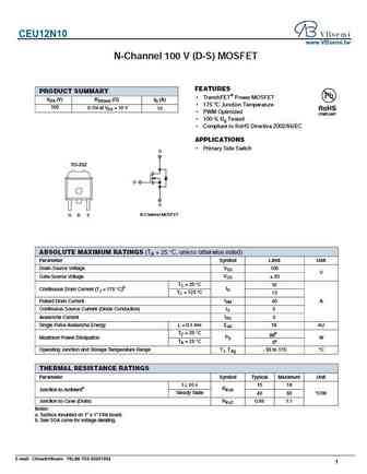
ceu12n10 ced12n10.pdf

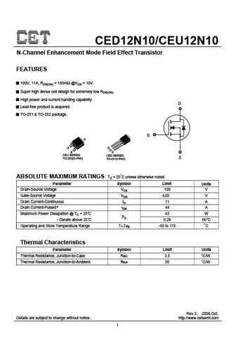
CED12N10/CEU12N10 N-Channel Enhancement Mode Field Effect Transistor FEATURES 100V, 11A, RDS(ON) = 180m @VGS = 10V. Super high dense cell design for extremely low RDS(ON). High power and current handing capability. D Lead free product is acquired. TO-251 & TO-252 package. G D G S CEU SERIES CED SERIES S TO-252(D-PAK) TO-251(I-PAK) ABSOLUTE MAXIMUM RATINGS Tc = 25 C unless o... See More ⇒
ced12n10 ceu12n10.pdf
CED12N10/CEU12N10 N-Channel Enhancement Mode Field Effect Transistor FEATURES 100V, 11A, RDS(ON) = 180m @VGS = 10V. Super high dense cell design for extremely low RDS(ON). High power and current handing capability. D Lead free product is acquired. TO-251 & TO-252 package. G D G S CEU SERIES CED SERIES S TO-252(D-PAK) TO-251(I-PAK) ABSOLUTE MAXIMUM RATINGS Tc = 25 C unless o... See More ⇒
ceu12n10l ced12n10l.pdf
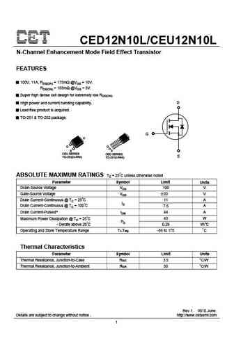
CED12N10L/CEU12N10L N-Channel Enhancement Mode Field Effect Transistor FEATURES 100V, 11A, RDS(ON) = 175m @VGS = 10V. RDS(ON) = 185m @VGS = 5V. Super high dense cell design for extremely low RDS(ON). High power and current handing capability. D Lead free product is acquired. TO-251 & TO-252 package. G D G S CEU SERIES CED SERIES S TO-252(D-PAK) TO-251(I-PAK) ABSOLUTE MA... See More ⇒
cs12n10.pdf
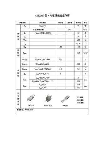
CS12N10 N PD TC=25 75 W 0.6 W/ ID VGS=10V,TC=25 12 A IDM 30 A VGS 20 V Tjm +150 Tstg -55 +150 RthJC 1.25 /W BVDSS VGS=0V,ID=0.25mA 100 V RDS on VGS=10V,ID=45A 0.18 VGS th VDS=VGS,ID=0.25mA... See More ⇒
ftk12n10s.pdf
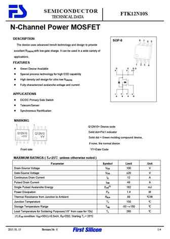
SEMICONDUCTOR FTK12N10S TECHNICAL DATA N-Channel Power MOSFET DESCRIPTION SOP-8 The device uses advanced trench technology and design to provide excellent RDS(ON) with low gate charge. It can be used in a wide variety of applications. FEATURES D D D D Green Device Available 8 6 5 7 Special process technology for high ESD capability High density cell design for ul... See More ⇒
blp12n10g-e.pdf
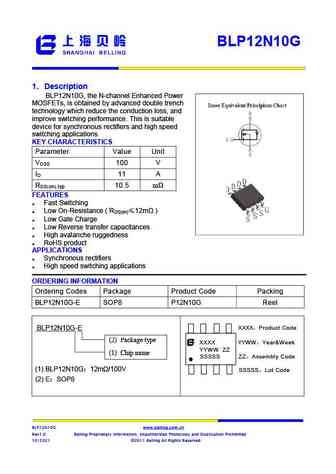
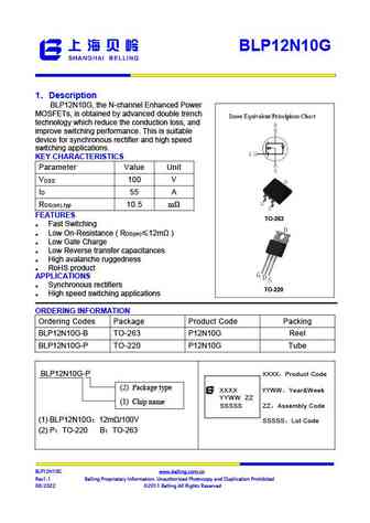
BLP12N10G Step-Down Converter , 1 Description BLP12N10G, the N-channel Enhanced Power MOSFETs, is obtained by advanced double trench technology which reduce the conduction loss, and improve switching performance. This is suitable device for synchronous rectifiers and high speed switching applications. KEY CHARACTERISTICS Parameter Value Unit V 100 V DSS I 11 A D ... See More ⇒
blp12n10gl-q.pdf
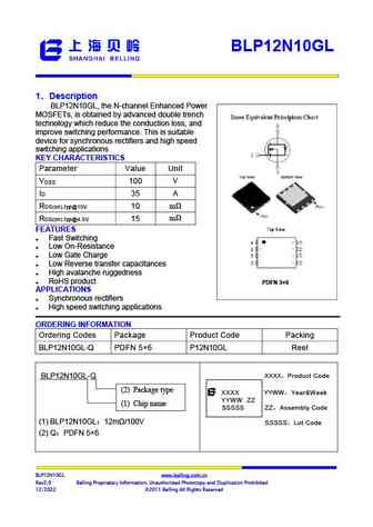
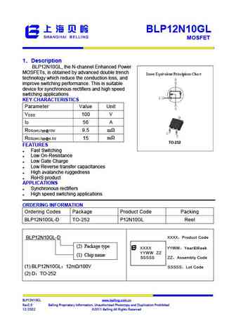
BLP12N10GL Step-Down Converter , 1 Description BLP12N10GL, the N-channel Enhanced Power MOSFETs, is obtained by advanced double trench technology which reduce the conduction loss, and improve switching performance. This is suitable device for synchronous rectifiers and high speed switching applications. KEY CHARACTERISTICS Parameter Value Unit V 100 V DSS I 35 A ... See More ⇒
blp12n10g-b blp12n10g-p.pdf
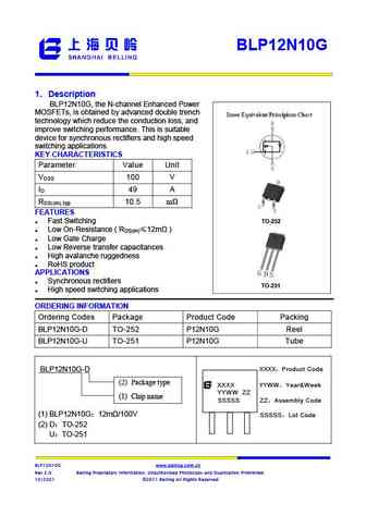
BLP12N10G Step-Down Converter , 1 Description BLP12N10G, the N-channel Enhanced Power MOSFETs, is obtained by advanced double trench technology which reduce the conduction loss, and improve switching performance. This is suitable device for synchronous rectifier and high speed switching applications. KEY CHARACTERISTICS Parameter Value Unit V 100 V DSS I 55 A D ... See More ⇒
blp12n10gl-d.pdf
BLP12N10GL MOSFET Step-Down Converter , 1 Description BLP12N10GL, the N-channel Enhanced Power MOSFETs, is obtained by advanced double trench technology which reduce the conduction loss, and improve switching performance. This is suitable device for synchronous rectifiers and high speed switching applications. KEY CHARACTERISTICS Parameter Value Unit V 100 V DSS ... See More ⇒
blp12n10g-q.pdf
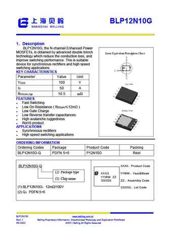
BLP12N10G Step-Down Converter , 1 Description BLP12N10G, the N-channel Enhanced Power MOSFETs, is obtained by advanced double trench technology which reduce the conduction loss, and improve switching performance. This is suitable device for synchronous rectifiers and high speed switching applications. KEY CHARACTERISTICS Parameter Value Unit V 100 V DSS I 50 A D ... See More ⇒
blp12n10g-d blp12n10g-u.pdf
BLP12N10G Step-Down Converter , 1 Description BLP12N10G, the N-channel Enhanced Power MOSFETs, is obtained by advanced double trench technology which reduce the conduction loss, and improve switching performance. This is suitable device for synchronous rectifiers and high speed switching applications. KEY CHARACTERISTICS Parameter Value Unit V 100 V DSS I 49 A D ... See More ⇒
chm12n10pagp.pdf
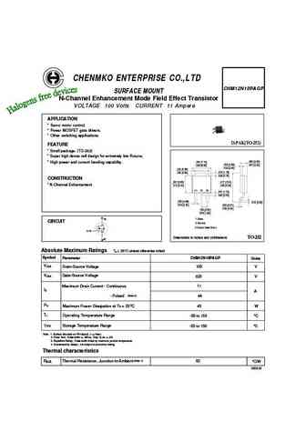
CHENMKO ENTERPRISE CO.,LTD CHM12N10PAGP SURFACE MOUNT N-Channel Enhancement Mode Field Effect Transistor VOLTAGE 100 Volts CURRENT 11 Ampere APPLICATION * Servo motor control. * Power MOSFET gate drivers. * Other switching applications. D-PAK(TO-252) FEATURE * Small package. (TO-252) * Super high dense cell design for extremely low RDS(ON). .094 (2.40) .280 (7.10) * High powe... See More ⇒
ncep12n10aq.pdf
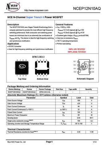
NCEP12N10AQ http //www.ncepower.com NCE N-Channel Super Trench II Power MOSFET Description General Features The NCEP12N10AQ uses Super Trench II technology that is VDS =100V,ID =46A uniquely optimized to provide the most efficient high frequency RDS(ON)=12.1m (typical) @ VGS=10V switching performance. Both conduction and switching power RDS(ON)=15.8m (typical) @ VGS=4.5V ... See More ⇒
wvm12n10.pdf
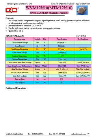
Shaanxi Qunli Electric Co., Ltd Add. No. 1 Qunli Road,Baoji City,Shaanxi,China WVM12N10(MTM12N10) Power MOSFET(N-channel) Transistor Features 1. It s voltage control component with good input impedance, small starting power dissipation, wide area of safe operation, good temperature stability. 2. Implementation of standards QZJ840611 3. Use for high speed switch, circuit of powe... See More ⇒
sl12n10.pdf
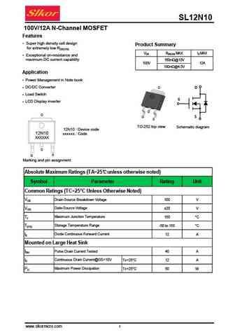
SL12N10 100V/12A N-Channel MOSFET Features Super high density cell design Product Summary for extremely low RDS(ON) VDS RDS(ON) MAX ID MAX Exceptional on-resistance and maximum DC current capability 160m @10V D2 S1 100V 12A D1 180m @4.5V Application Power Management in Note book DC/DC Converter D Load Switch LCD Display inverter D D G S... See More ⇒
sl12n100t sl12n100k sl12n100 sl12n100f.pdf
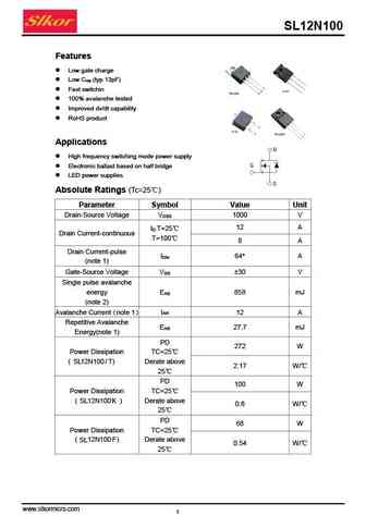
SL12N100 Features Low gate charge Low C (typ 13pF) rss Fast switchin 100% avalanche tested Improved dv/dt capability RoHS product Applications High frequency switching mode power supply Electronic ballast based on half bridge LED power supplies Absolute Ratings (Tc=25 ) Parameter Symbol Value Unit Drain-Source Voltage V 1000 V DSS 12 A I T... See More ⇒
st12n10d.pdf
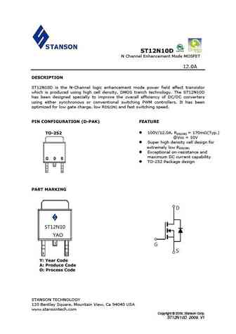
ST12N10D N Channel Enhancement Mode MOSFET 12.0A DESCRIPTION ST12N10D is the N-Channel logic enhancement mode power field effect transistor which is produced using high cell density, DMOS trench technology. The ST12N10D has been designed specially to improve the overall efficiency of DC/DC converters using either synchronous or conventional switching PWM controllers. It has been... See More ⇒
wml12n105c2 wmm12n105c2 wmn12n105c2 wmj12n105c2 wmk12n105c2.pdf
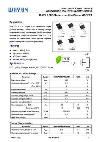
WML12N105C2, WMM12N105C2 WMN12N105C2, WMJ12N105C2, WMK12N105C2 1050V 0.68 Super Junction Power MOSFET Description WMOSTM C2 is Wayon s 2nd generation super junction MOSFET family that is utilizing charge S balance technology for extremely low on-resistance S D D G G S D G and low gate charge performance. WMOSTM C2 is TO-220F TO-262 TO-220 suitable for applic... See More ⇒
wml12n100c2 wmm12n100c2 wmn12n100c2 wmj12n100c2 wmk12n100c2.pdf
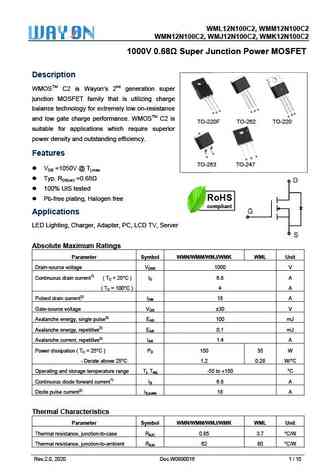
WML12N100C2, WMM C2 W M12N100C WMN12N WMJ12N10 K12N100C N100C2, W 00C2, WMK C2 1000V 0.68 S unction Power M T Super Ju MOSFET Descrip ption WMOSTM C2 is Wa 2nd generation super ayon s n junction MOSFET fa that is utilizing charge M amily S balance te or extremely esistance echnology fo y low on-re S D D G G G S D G and low ga charge performanc WMOSTM C... See More ⇒
hsu12n10.pdf
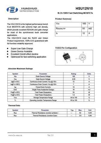
HSU12N10 N-Ch 100V Fast Switching MOSFETs Description Product Summary VDS 100 V The HSU12N10 is the highest performance trench N-ch MOSFETs with extreme high cell density, RDS(ON),TYP 93 m which provide excellent RDSON and gate charge for most of the synchronous buck converter ID 12 A applications . The HSU12N10 meet the RoHS and Green Product requirement, 100% EAS gua... See More ⇒
ptd12n10.pdf
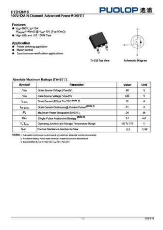
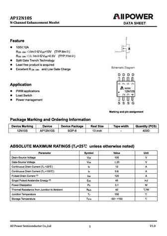
PTD12N10 100V/12A N-Channel Advanced PowerMOSFET Features VDS=100V; ID=12A RDS(ON)... See More ⇒
agm12n10d.pdf
AGM12N10D Characteristics Curve Typ. output characteristics Typ. drain-source on resistance I =f(V ) R =f(I ) D DS DS(on) D Typ. transfer characteristics Drain-source on-state resistance I =f(V ) R =f(T );I =20A; V =10V D GS DS(on) j D GS www.agm-mos.com 3 VER2.71 AGM12N10D Gate Threshold Voltage Drain-source breakdown voltage V =f(T ); I =250uA V =f(T ); I =250uA TH j... See More ⇒
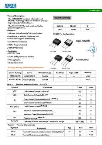
agmh12n10c.pdf
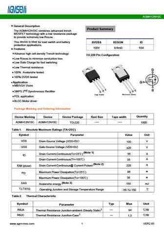
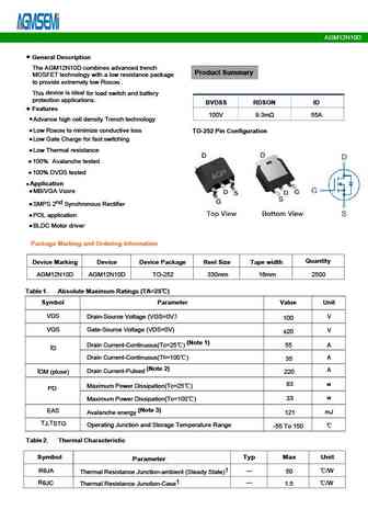
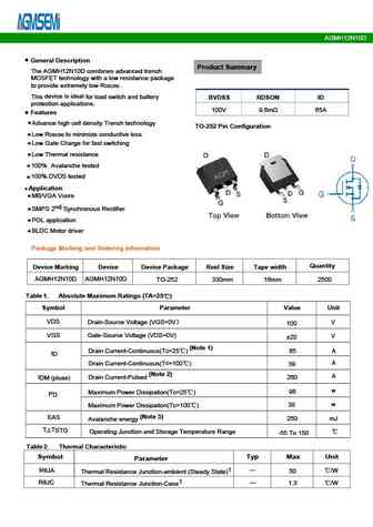
AGMH12N10C General Description Product Summary The AGMH12N10C combines advanced trench MOSFET technology with a low resistance package to provide extremely low R . DS(ON) device is ideal This for load switch and battery BVDSS RDSON ID protection applications. 100V 9.6m 55A Features Advance high cell density Trench technology TO-220 Pin Configuration Low R to m... See More ⇒
agm12n10mna.pdf
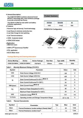
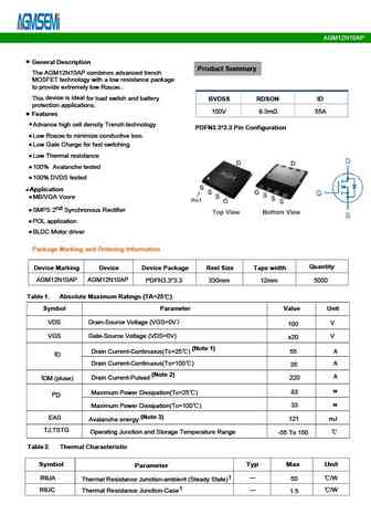
AGM12N10MNA General Description Product Summary The AGM12N10MNA combines advanced trench MOSFET technology with a low resistance package to provide extremely low R . DS(ON) device is ideal This for load switch and battery BVDSS RDSON ID protection applications. 100V 11m 55A Features Advance high cell density Trench technology PDFN5*6 Pin Configuration Low R to... See More ⇒
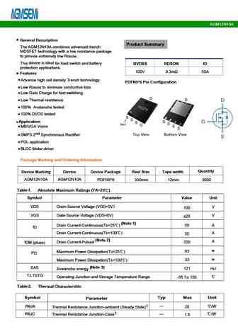
agm12n10a.pdf
AGM12N10A Characteristics Curve Typ. output characteristics Typ. drain-source on resistance I =f(V ) R =f(I ) D DS DS(on) D Typ. transfer characteristics Drain-source on-state resistance I =f(V ) R =f(T );I =20A; V =10V D GS DS(on) j D GS www.agm-mos.com 3 VER2.71 AGM12N10A Gate Threshold Voltage Drain-source breakdown voltage V =f(T ); I =250uA V =f(T ); I =250uA TH j... See More ⇒
agmh12n10i.pdf
AGMH12N10I Characteristics Curve Typ. output characteristics Typ. drain-source on resistance I =f(V ) R =f(I ) D DS DS(on) D Typ. transfer characteristics Drain-source on-state resistance I =f(V ) R =f(T );I =20A; V =10V D GS DS(on) j D GS www.agm-mos.com 3 VER2.71 AGMH12N10I Gate Threshold Voltage Drain-source breakdown voltage V =f(T ); I =250uA V =f(T ); I =250uA TH... See More ⇒
agmh12n10d.pdf
AGMH12N10D Characteristics Curve Typ. output characteristics Typ. drain-source on resistance I =f(V ) R =f(I ) D DS DS(on) D Typ. transfer characteristics Drain-source on-state resistance I =f(V ) R =f(T );I =20A; V =10V D GS DS(on) j D GS www.agm-mos.com 3 VER2.71 AGMH12N10D AGMH12N10D Gate Threshold Voltage Drain-source breakdown voltage V =f(T ); I =250uA V =f(T ); I... See More ⇒
agm12n10ap.pdf
AGM12N10AP Table 3. Electrical Characteristics (TJ=25 unless otherwise noted) Symbol Parameter Conditions Min Typ Max Unit On/Off States BV Drain-Source Breakdown Voltage V =0V I =250 A 100 -- -- V GS D DSS Zero Gate Voltage Drain Current V =100V,V =0V -- -- 1.0 A DS GS I DSS V = 20V,V =0V -- -- nA GS DS IGSS Gate-Body Leakage Current 100 VGS(th) Gate Threshold Volt... See More ⇒
wsf12n10.pdf
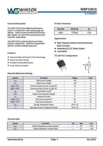
WSF12N10 N-Ch MOSFET Product Summery General Description The WSF12N10 is the highest performance BVDSS RDSON ID trench N-ch MOSFET with extreme high cell 175m 12A density , which provide excellent RDSON and 100V gate charge for most of the synchronous buck converter applications . Applications The WSF12N10 meet the RoHS and Green High Frequency Point-of-Load Synchrono... See More ⇒
st12n10d.pdf

ST12N10D www.VBsemi.tw N-Channel 100 V (D-S) MOSFET FEATURES PRODUCT SUMMARY TrenchFET Power MOSFET VDS (V) RDS(on) ( )ID (A) 175 C Junction Temperature 100 0.11 4 at VGS = 10 V 15 PWM Optimized 100 % Rg Tested Compliant to RoHS Directive 2002/95/EC APPLICATIONS Primary Side Switch D TO-252 G S G D S N-Channel MOSFET ABSOLUTE MAXIMUM RATINGS... See More ⇒
ntd12n10-1g.pdf
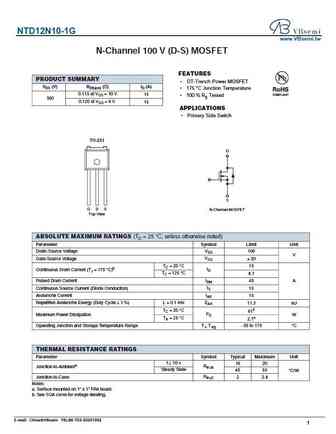
NTD12N10-1G www.VBsemi.tw N-Channel 100 V (D-S) MOSFET FEATURES PRODUCT SUMMARY DT-Trench Power MOSFET VDS (V) RDS(on) ( )ID (A) 175 C Junction Temperature 0.115 at VGS = 10 V 15 100 % Rg Tested 100 0.120 at VGS = 6 V 15 APPLICATIONS Primary Side Switch TO-251 D G S G D S N-Channel MOSFET Top View ABSOLUTE MAXIMUM RATINGS (TC = 25 C, unless otherwi... See More ⇒
ceu12n10.pdf
CEU12N10 www.VBsemi.tw N-Channel 100 V (D-S) MOSFET FEATURES PRODUCT SUMMARY TrenchFET Power MOSFET VDS (V) RDS(on) ( )ID (A) 175 C Junction Temperature 100 0.11 4 at VGS = 10 V 15 PWM Optimized 100 % Rg Tested Compliant to RoHS Directive 2002/95/EC APPLICATIONS Primary Side Switch D TO-252 G S G D S N-Channel MOSFET ABSOLUTE MAXIMUM RATINGS... See More ⇒
mtp12n10l.pdf
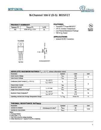
MTP12N10L www.VBsemi.com N-Channel 100-V (D-S) MOSFET FEATURES PRODUCT SUMMARY TrenchFET Power MOSFET V(BR)DSS (V) RDS(on) ( )ID (A) 175 C Junction Temperature RoHS 0.092 at VGS = 10 V 100 18 COMPLIANT Low Thermal Resistance Package 100 % Rg Tested APPLICATIONS Isolated DC/DC Converters TO-220AB D G S G D S N-Channel MOSFET Top View ABSOLUTE M... See More ⇒
cmu12n10.pdf
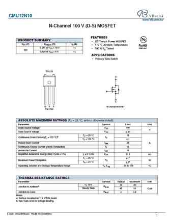
CMU12N10 www.VBsemi.tw N-Channel 100 V (D-S) MOSFET FEATURES PRODUCT SUMMARY DT-Trench Power MOSFET VDS (V) RDS(on) ( )ID (A) 175 C Junction Temperature 0.115 at VGS = 10 V 15 100 % Rg Tested 100 0.120 at VGS = 6 V 15 APPLICATIONS Primary Side Switch TO-251 D G S G D S N-Channel MOSFET Top View ABSOLUTE MAXIMUM RATINGS (TC = 25 C, unless otherwise... See More ⇒
mtp12n10e.pdf
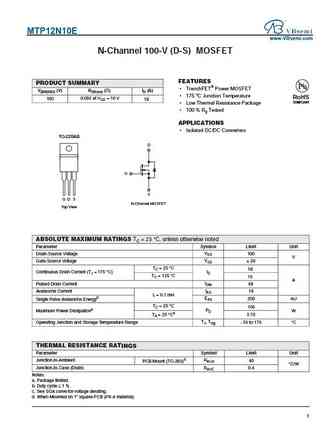
MTP12N10E www.VBsemi.com N-Channel 100-V (D-S) MOSFET FEATURES PRODUCT SUMMARY TrenchFET Power MOSFET V(BR)DSS (V) RDS(on) ( )ID (A) 175 C Junction Temperature RoHS 0.092 at VGS = 10 V 100 18 COMPLIANT Low Thermal Resistance Package 100 % Rg Tested APPLICATIONS Isolated DC/DC Converters TO-220AB D G S G D S N-Channel MOSFET Top View ABSOLUTE M... See More ⇒
ced12n10l.pdf
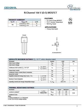
CED12N10L www.VBsemi.tw N-Channel 100 V (D-S) MOSFET FEATURES PRODUCT SUMMARY DT-Trench Power MOSFET VDS (V) RDS(on) ( )ID (A) 175 C Junction Temperature 0.115 at VGS = 10 V 15 100 % Rg Tested 100 0.120 at VGS = 6 V 15 APPLICATIONS Primary Side Switch TO-251 D G S G D S N-Channel MOSFET Top View ABSOLUTE MAXIMUM RATINGS (TC = 25 C, unless otherwis... See More ⇒
vbze12n10.pdf
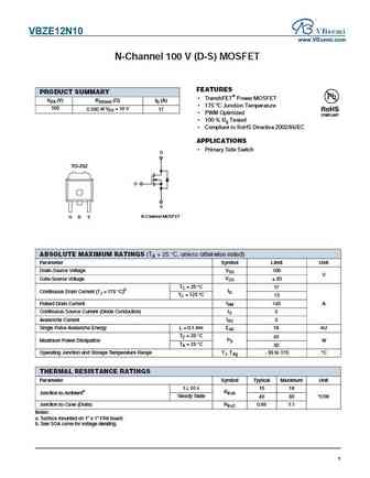
VBZE12N10 www.VBsemi.com N-Channel 100 V (D-S) MOSFET FEATURES PRODUCT SUMMARY TrenchFET Power MOSFET VDS (V) RDS(on) ( )ID (A) 175 C Junction Temperature 100 at VGS = 10 V 0.090 17 PWM Optimized 100 % Rg Tested Compliant to RoHS Directive 2002/95/EC APPLICATIONS Primary Side Switch D TO-252 G S G D S N-Channel MOSFET ABSOLUTE MAXIMUM RATINGS... See More ⇒
ced12n10.pdf

CED12N10 www.VBsemi.tw N-Channel 100 V (D-S) MOSFET FEATURES PRODUCT SUMMARY DT-Trench Power MOSFET VDS (V) RDS(on) ( )ID (A) 175 C Junction Temperature 0.115 at VGS = 10 V 15 100 % Rg Tested 100 0.120 at VGS = 6 V 15 APPLICATIONS Primary Side Switch TO-251 D G S G D S N-Channel MOSFET Top View ABSOLUTE MAXIMUM RATINGS (TC = 25 C, unless otherwise... See More ⇒
tsg12n10at.pdf
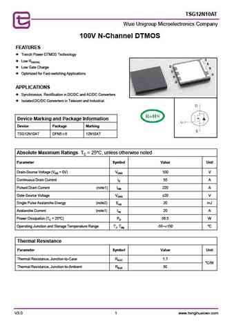
TSG12N10AT Wuxi Unigroup Microelectronics Company 100V N-Channel DTMOS FEATURES Trench Power DTMOS Technology Low RDS(ON) Low Gate Charge Optimized for Fast-switching Applications APPLICATIONS Synchronous Rectification in DC/DC and AC/DC Converters Isolated DC/DC Converters in Telecom and Industrial Device Marking and Package Information Device P... See More ⇒
mdt12n10l.pdf
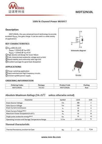
100V N-Channel Power MOSFET Description MDT12N10L, the uses advanced trench technology to provide excellent R , low gate charge. It can be used in a wide variety DS(ON) of applications KEY CHARACTERISTICS V =100V,ID=12A DS R ... See More ⇒
ap12n10y.pdf
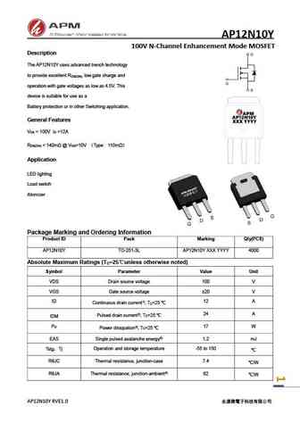
AP12N10Y 100V N-Channel Enhancement Mode MOSFET Description The AP12N10Y uses advanced trench technology to provide excellent R , low gate charge and DS(ON) operation with gate voltages as low as 4.5V. This device is suitable for use as a Battery protection or in other Switching application. General Features V = 100V I =12A DS D R ... See More ⇒
apg12n10d.pdf
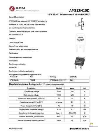
APG12N10D 100V N-SGT Enhancement Mode MOSFET General Description APG12N10D use advanced SGT MOSFET technology to provide low RDS(ON), low gate charge, fast switching and excellent avalanche characteristics. This device is specially designed to get better ruggedness and suitable to use in Features Low RDS(on) & FOM Extremely low switching loss Excellent stability and unifo... See More ⇒
Detailed specifications: 2N7002LL, 2N7002Z, 2N7002ZT, UF3055, UTD3055, 12N06, 12N06Z, 15N06, IRL3713, 15N20, 19N10, 22N20, 25N06, 25N10, 30N06, 50N06, 60N06
Keywords - 12N10 MOSFET specs
12N10 cross reference
12N10 equivalent finder
12N10 pdf lookup
12N10 substitution
12N10 replacement
Need a MOSFET replacement? Our guide shows you how to find a perfect substitute by comparing key parameters and specs
MOSFET Parameters. How They Affect Each Other
History: DSG140N12N3 | 2SJ113 | UF740
🌐 : EN ES РУ

LIST
Last Update
MOSFET: CEZC2P07 | CEZ2R05 | CEU3133 | CES2361 | CES2312A | CEP100N10L | CEM3425 | CEM3139 | CEM3133 | CEM3115
Popular searches
c3199 transistor | 2n2712 datasheet | 2sc2525 | tip73 | 2n3392 | 2n2369a | 2sc733 | a933 transistor