MTEB6N20J3 Specs and Replacement
Type Designator: MTEB6N20J3
Type of Transistor: MOSFET
Type of Control Channel: N-Channel
Absolute Maximum Ratings
Pd ⓘ - Maximum Power Dissipation: 50 W
|Vds|ⓘ - Maximum Drain-Source Voltage: 200 V
|Vgs|ⓘ - Maximum Gate-Source Voltage: 30 V
|Id| ⓘ - Maximum Drain Current: 8.3 A
Tj ⓘ - Maximum Junction Temperature: 150 °C
Electrical Characteristics
tr ⓘ - Rise Time: 12 nS
Cossⓘ - Output Capacitance: 42 pF
RDSonⓘ - Maximum Drain-Source On-State Resistance: 0.3 Ohm
Package: TO-252
MTEB6N20J3 substitution
- MOSFET ⓘ Cross-Reference Search
MTEB6N20J3 datasheet
mteb6n20j3.pdf
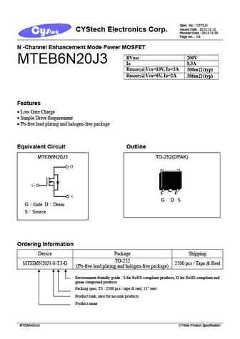
Spec. No. C875J3 Issued Date 2012.12.12 CYStech Electronics Corp. Revised Date 2013.12.30 Page No. 1/9 N -Channel Enhancement Mode Power MOSFET BVDSS 200V MTEB6N20J3 ID 8.3A RDS(ON)@VGS=10V, ID=3A 300m (typ) RDS(ON)@VGS=6V, ID=2A 306m (typ) Features Low Gate Charge Simple Drive Requirement Pb-free lead plating and halogen-free package Equivalent... See More ⇒
Detailed specifications: MTE65N20J3, MTEA0N10J3, MTEA0N10Q8, MTEA2N15L3, MTEA2N15Q8, MTEA6C15J4, MTEA6C15Q8, MTEB4N15J3, AOD4184A, MTED6N25J3, MTED6N25KJ3, MTEE2N20FP, MTEE2N20J3, MTEF1P15L3, MTEF1P15N6, MTEF1P15Q8, MTEF1P15V8
Keywords - MTEB6N20J3 MOSFET specs
MTEB6N20J3 cross reference
MTEB6N20J3 equivalent finder
MTEB6N20J3 pdf lookup
MTEB6N20J3 substitution
MTEB6N20J3 replacement
Can't find your MOSFET? Learn how to find a substitute transistor by analyzing voltage, current and package compatibility
🌐 : EN ES РУ

LIST
Last Update
MOSFET: AKF30N5P0SX | AKF30N10S | AKF20P45D | CM4407 | CM3407 | CM3400 | SVF11N65F | SVF11N65T | FKBB3105 | EHBA036R1
Popular searches
d2390 datasheet | 2sa750 replacement | 2sc984 replacement | a1046 transistor | hy19p03 | 2sk2749 | c2577 transistor | k3563 transistor