SSP7N60B Datasheet. Specs and Replacement
Type Designator: SSP7N60B 📄📄
Type of Transistor: MOSFET
Type of Control Channel: N-Channel
Absolute Maximum Ratings
Pd ⓘ - Maximum Power Dissipation: 147 W
|Vds|ⓘ - Maximum Drain-Source Voltage: 600 V
|Vgs|ⓘ - Maximum Gate-Source Voltage: 30 V
|Id| ⓘ - Maximum Drain Current: 7 A
Tj ⓘ - Maximum Junction Temperature: 150 °C
Electrical Characteristics
tr ⓘ - Rise Time: 80 nS
Cossⓘ - Output Capacitance: 115 pF
RDSonⓘ - Maximum Drain-Source On-State Resistance: 1.2 Ohm
Package: TO220
📄📄 Copy
SSP7N60B substitution
- MOSFET ⓘ Cross-Reference Search
SSP7N60B datasheet
ssp7n60b sss7n60b.pdf
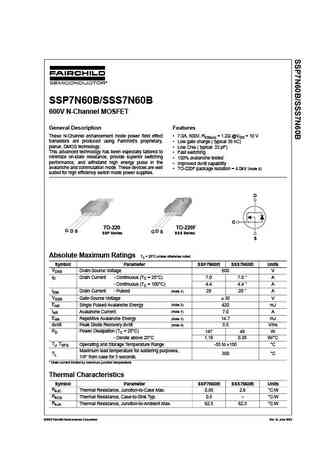
SSP7N60B/SSS7N60B 600V N-Channel MOSFET General Description Features These N-Channel enhancement mode power field effect 7.0A, 600V, RDS(on) = 1.2 @VGS = 10 V transistors are produced using Fairchild s proprietary, Low gate charge ( typical 38 nC) planar, DMOS technology. Low Crss ( typical 23 pF) This advanced technology has been especially tailored to Fast switchi... See More ⇒
ssp7n60a.pdf

Advanced Power MOSFET FEATURES BVDSS = 600 V Avalanche Rugged Technology RDS(on) = 1.2 Rugged Gate Oxide Technology Lower Input Capacitance ID = 7 A Improved Gate Charge Extended Safe Operating Area Lower Leakage Current 25 A (Max.) @ VDS = 600V Lower RDS(ON) 0.977 (Typ.) 1 2 3 1.Gate 2. Drain 3. Source Absolute Maximum Ratings Symbol Characteristic Valu... See More ⇒
ssp7n80a.pdf
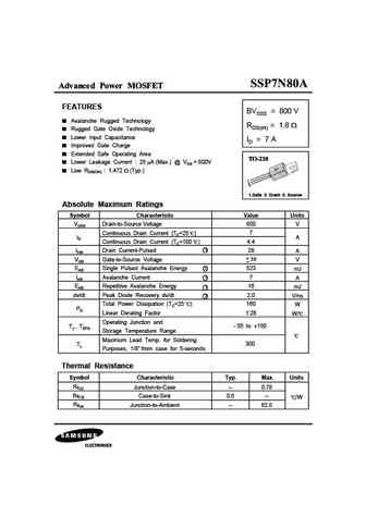
Advanced Power MOSFET FEATURES BVDSS = 800 V Avalanche Rugged Technology RDS(on) = 1.8 Rugged Gate Oxide Technology Lower Input Capacitance ID = 7 A Improved Gate Charge Extended Safe Operating Area Lower Leakage Current 25 A (Max.) @ VDS = 800V Low RDS(ON) 1.472 (Typ.) 1 2 3 1.Gate 2. Drain 3. Source Absolute Maximum Ratings Symbol Characteristic Value ... See More ⇒
Detailed specifications: FTD04N60A, FTU04N60B, FTD04N60B, FTU04N65C, FTD04N65C, FTU06N70C, FTD06N70C, 2SK1487, AON6426, SSS7N60B, SSM40N03P, IRF830B, IRFS830B, CLY2, 2SK2369, 2SK2370, 2SK2357
Keywords - SSP7N60B MOSFET specs
SSP7N60B cross reference
SSP7N60B equivalent finder
SSP7N60B pdf lookup
SSP7N60B substitution
SSP7N60B replacement
Need a MOSFET replacement? Our guide shows you how to find a perfect substitute by comparing key parameters and specs
MOSFET Parameters. How They Affect Each Other
🌐 : EN ES РУ

LIST
Last Update
MOSFET: BC2301 | BC1012W | BC1012T | BC1012 | 2SK3019WT | 2SK3019W | 2SK3018WT | CS95118 | CS85105A | CS75N45
Popular searches
tip41c | irfp460 | irfz44n mosfet | lm317t datasheet | irf540 | bc337 | ksc1845 | c1815 transistor