SSF2112H2 Specs and Replacement
Type Designator: SSF2112H2
Type of Transistor: MOSFET
Type of Control Channel: N-Channel
Absolute Maximum Ratings
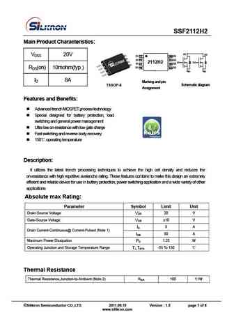
Pd ⓘ - Maximum Power Dissipation: 1.25 W
|Vds|ⓘ - Maximum Drain-Source Voltage: 20 V
|Vgs|ⓘ - Maximum Gate-Source Voltage: 10 V
|Id| ⓘ - Maximum Drain Current: 8 A
Tj ⓘ - Maximum Junction Temperature: 150 °C
Electrical Characteristics
tr ⓘ - Rise Time: 4.8 nS
Cossⓘ - Output Capacitance: 229 pF
RDSonⓘ - Maximum Drain-Source On-State Resistance: 0.0125 Ohm
Package: TSSOP8
SSF2112H2 substitution
- MOSFET ⓘ Cross-Reference Search
SSF2112H2 datasheet
ssf2112h2.pdf
SSF2112H2 Main Product Characteristics D1 D2 VDSS 20V D1 D2 S1 S2 G1 G2 2112H2 8205A S1 S2 G1 G2 RDS(on) 10mohm(typ.) S1 S2 ID 8A Marking and pin Schematic diagram TSSOP-8 Assignment Features and Benefits Advanced trench MOSFET process technology Special designed for buttery protection, load switching and general power management Ultra low on-re... See More ⇒
ssf2116ej3.pdf
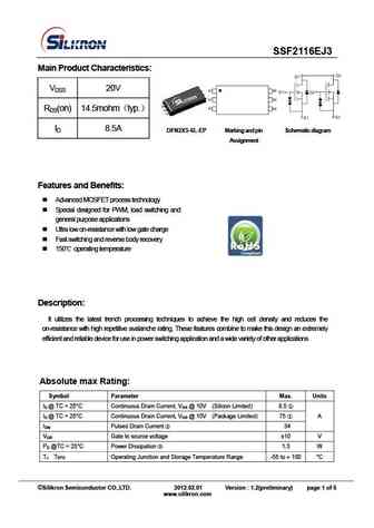
SSF2116EJ3 Main Product Characteristics VDSS 20V RDS(on) 14.5mohm typ. ID 8.5A DFN2X5-6L-EP Marking and pin Schematic diagram Assignment Features and Benefits Advanced MOSFET process technology Special designed for PWM, load switching and general purpose applications Ultra low on-resistance with low gate charge Fast switching and reverse body recov... See More ⇒
ssf2145ch6.pdf
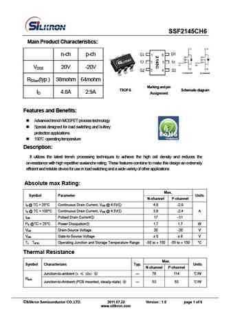
SSF2145CH6 Main Product Characteristics n-ch p-ch VDSS 20V -20V RDSon(typ.) 38mohm 64mohm Marking and pin TSOP-6 Schematic diagram ID 4.8A 2.9A Assignment Features and Benefits Advanced trench MOSFET process technology Special designed for load switching and buttery protection applications 150 operating temperature Description It utilizes the l... See More ⇒
ssf2129h3.pdf
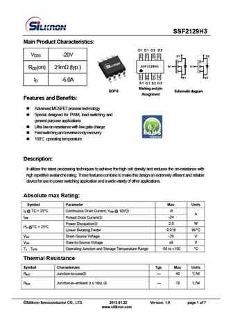
SSF2129H3 Main Product Characteristics VDSS -20V D1 D2 G1 G2 RDS(on) 21m (typ.) S1 S2 ID -6.0A Marking and pin SOP-8 S che matic diagram Assignment Features and Benefits Advanced MOSFET process technology Special designed for PWM, load switching and general purpose applications Ultra low on-resistance with low gate charge Fast switching and re... See More ⇒
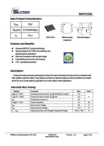
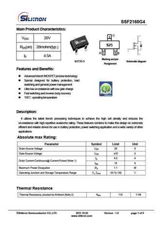
Detailed specifications: SSF1N80G5, SSF1N90D, SSF20N50UH, SSF20N60H, SSF20NS60, SSF20NS60F, SSF20NS65, SSF20NS65F, IRF640N, SSF2116EJ3, SSF2122E, SSF2129H3, SSF2145CH6, SSF2160G4, SSF2300, SSF2300A, SSF2300B
Keywords - SSF2112H2 MOSFET specs
SSF2112H2 cross reference
SSF2112H2 equivalent finder
SSF2112H2 pdf lookup
SSF2112H2 substitution
SSF2112H2 replacement
Can't find your MOSFET? Learn how to find a substitute transistor by analyzing voltage, current and package compatibility
🌐 : EN ES РУ
LIST
Last Update
MOSFET: FTF30P35D | FTF25N35DHVT | FTF15N35D | FTE15C35G | FTP02P15G | FTE02P15G | AKF30N5P0SX | AKF30N10S | AKF20P45D | CM4407
Popular searches
a1273 transistor | 2sc1384 equivalent | 2sd786 | a940 transistor | 2sc1815 replacement | 2sc2383 | c3198 transistor | irfb3607pbf datasheet
