P9006EVG Datasheet. Specs and Replacement
Type Designator: P9006EVG 📄📄
Type of Transistor: MOSFET
Type of Control Channel: P-Channel
Absolute Maximum Ratings
Pd ⓘ - Maximum Power Dissipation: 2.5 W
|Vds|ⓘ - Maximum Drain-Source Voltage: 60 V
|Vgs|ⓘ - Maximum Gate-Source Voltage: 20 V
|Id| ⓘ - Maximum Drain Current: 4.5 A
Tj ⓘ - Maximum Junction Temperature: 150 °C
Electrical Characteristics
tr ⓘ - Rise Time: 10 nS
Cossⓘ - Output Capacitance: 90 pF
RDSonⓘ - Maximum Drain-Source On-State Resistance: 0.09 Ohm
Package: SOP8
📄📄 Copy
P9006EVG substitution
- MOSFET ⓘ Cross-Reference Search
P9006EVG datasheet
p9006evg.pdf

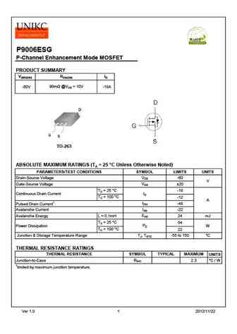
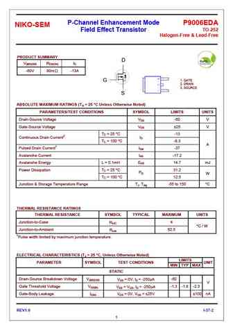
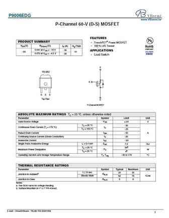
P9006EVG P-Channel Enhancement Mode MOSFET PRODUCT SUMMARY V(BR)DSS RDS(ON) ID -60V 90m @VGS = -10V -4.5A SOP- 08 ABSOLUTE MAXIMUM RATINGS (TA = 25 C Unless Otherwise Noted) ( ) PARAMETERS/TEST CONDITIONS SYMBOL LIMITS UNITS VDS Drain-Source Voltage -60 V VGS Gate-Source Voltage 20 TA = 25 C -4.5 ID Continuous Drain Current TA = 70 C A -3.5 IDM -20 Pulsed Drain ... See More ⇒
p9006evg.pdf
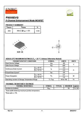
P9006EVG P-Channel Enhancement Mode MOSFET PRODUCT SUMMARY V(BR)DSS RDS(ON) ID -60V 90m @VGS = -10V -4.5A SOP- 08 ABSOLUTE MAXIMUM RATINGS (TA = 25 C Unless Otherwise Noted) ( ) PARAMETERS/TEST CONDITIONS SYMBOL LIMITS UNITS VDS Drain-Source Voltage -60 V VGS Gate-Source Voltage 20 TA = 25 C -4.5 ID Continuous Drain Current TA = 70 C A -3.5 IDM -20 Pulsed Drain ... See More ⇒
p9006eva.pdf
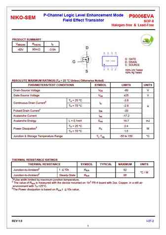
P-Channel Logic Level Enhancement Mode P9006EVA NIKO-SEM Field Effect Transistor SOP-8 Halogen-free & Lead-Free PRODUCT SUMMARY V(BR)DSS RDS(ON) ID D 90m -3.6A -60V G GATE G D DRAIN S SOURCE 100% UIS Tested S 100% Rg Tested ABSOLUTE MAXIMUM RATINGS (TA = 25 C Unless Otherwise Noted) PARAMETERS/TEST CONDITIONS SYMBOL LIMITS UNITS Drain-Source Volta... See More ⇒
mtp9006e3.pdf
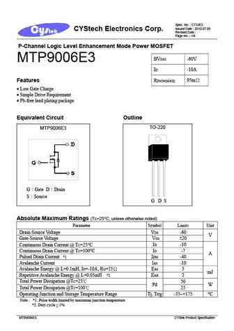
Spec. No. C733E3 Issued Date 2010.07.09 CYStech Electronics Corp. Revised Date Page No. 1/6 P-Channel Logic Level Enhancement Mode Power MOSFET BVDSS -60V MTP9006E3 ID -10A 95m Features RDSON(MAX) Low Gate Charge Simple Drive Requirement Pb-free lead plating package Equivalent Circuit Outline TO-220 MTP9006E3 G Gate D Drain S Source... See More ⇒
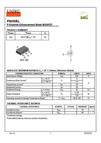
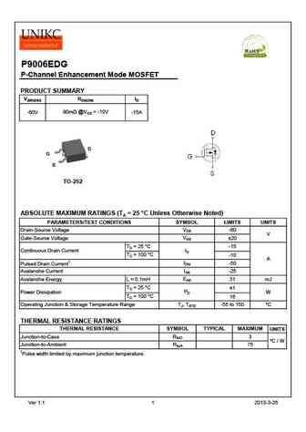
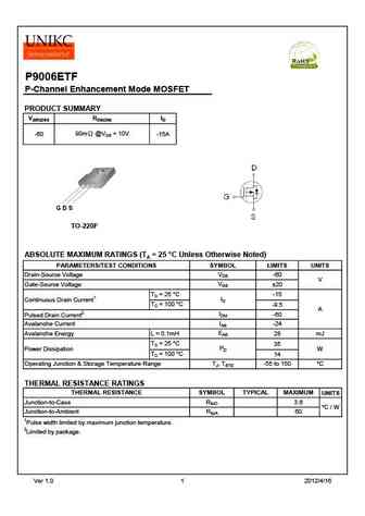
Detailed specifications: P06P03LCGA, P06P03LDG, P06P03LVG, P9006EDG, P9006EI, P9006EL, P9006ESG, P9006ETF, IRF640, P0703BD, P0703ED, P0703EV, P0765ATF, P0765GTF, P0765GTFS, P0770EI, P0770EIS
Keywords - P9006EVG MOSFET specs
P9006EVG cross reference
P9006EVG equivalent finder
P9006EVG pdf lookup
P9006EVG substitution
P9006EVG replacement
Step-by-step guide to finding a MOSFET replacement. Cross-reference parts and ensure compatibility for your repair or project.
MOSFET Parameters. How They Affect Each Other
🌐 : EN ES РУ

LIST
Last Update
MOSFET: CS95118 | CS85105A | CS75N45 | CS72N12 | CS55N50 | CS48N75A | CS40N27 | MSQ60P04D | MSQ40P07D | MSQ30P40D
Popular searches
2sa1837 | ksc1845 transistor | irf630 datasheet | mpsa13 equivalent | c5198 | 2sc1969 transistor | bcy21 | s8550 datasheet