P261AFEA Specs and Replacement
Type Designator: P261AFEA
Type of Transistor: MOSFET
Type of Control Channel: P-Channel
Absolute Maximum Ratings
Pd ⓘ - Maximum Power Dissipation: 2 W
|Vds|ⓘ - Maximum Drain-Source Voltage: 12 V
|Vgs|ⓘ - Maximum Gate-Source Voltage: 8 V
|Id| ⓘ - Maximum Drain Current: 9 A
Tj ⓘ - Maximum Junction Temperature: 150 °C
Electrical Characteristics
tr ⓘ - Rise Time: 70 nS
Cossⓘ - Output Capacitance: 599 pF
RDSonⓘ - Maximum Drain-Source On-State Resistance: 0.02 Ohm
Package: PDFN3X3P
P261AFEA substitution
- MOSFET ⓘ Cross-Reference Search
P261AFEA datasheet
p261afea.pdf
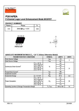
P261AFEA P-Channel Logic Level Enhancement Mode MOSFET PRODUCT SUMMARY V(BR)DSS RDS(ON) ID 20m @VGS = -4.5V -12V -32A PDFN 3x3P ABSOLUTE MAXIMUM RATINGS (TA = 25 C Unless Otherwise Noted) PARAMETERS/TEST CONDITIONS SYMBOL LIMITS UNITS VDS Drain-Source Voltage -12 V VGS Gate-Source Voltage 8 TC = 25 C -32 TC = 100 C -20 ID Continuous Drain Current2 TA = 25... See More ⇒
p261alv.pdf
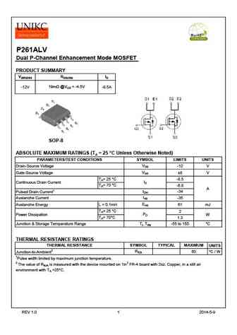
P261ALV Dual P-Channel Enhancement Mode MOSFET PRODUCT SUMMARY V(BR)DSS RDS(ON) ID 19m @VGS = -4.5V -12V -8.5A SOP-8 ABSOLUTE MAXIMUM RATINGS (TA = 25 C Unless Otherwise Noted) PARAMETERS/TEST CONDITIONS SYMBOL LIMITS UNITS VDS Drain-Source Voltage -12 V VGS Gate-Source Voltage 8 V TA= 25 C -8.5 ID Continuous Drain Current TA= 70 C -6.8 A IDM -34 Pulsed Dra... See More ⇒
Detailed specifications: P2610AI, P2610ATFG, P2610ATG, P2610BD, P2610BS, P2610BT, P2615ATFG, P2615ATG, AO3401, P261ALV, P1810ATX, P1820AD, P1820BD, P1825AD, P1825AT, P2003BDG, P3504BD
Keywords - P261AFEA MOSFET specs
P261AFEA cross reference
P261AFEA equivalent finder
P261AFEA pdf lookup
P261AFEA substitution
P261AFEA replacement
Learn how to find the right MOSFET substitute. A guide to cross-reference, check specs and replace MOSFETs in your circuits.
