PJ614DA Datasheet. Specs and Replacement
Type Designator: PJ614DA 📄📄
Type of Transistor: MOSFET
Type of Control Channel: N-Channel
Absolute Maximum Ratings
Pd ⓘ - Maximum Power Dissipation: 1.7 W
|Vds|ⓘ - Maximum Drain-Source Voltage: 20 V
|Vgs|ⓘ - Maximum Gate-Source Voltage: 10 V
|Id| ⓘ - Maximum Drain Current: 9 A
Tj ⓘ - Maximum Junction Temperature: 150 °C
Electrical Characteristics
tr ⓘ - Rise Time: 32 nS
Cossⓘ - Output Capacitance: 214 pF
RDSonⓘ - Maximum Drain-Source On-State Resistance: 0.0125 Ohm
Package: JLEAD
📄📄 Copy
PJ614DA substitution
- MOSFET ⓘ Cross-Reference Search
PJ614DA datasheet
pj614da.pdf
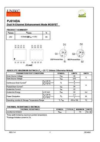
PJ614DA Dual N-Channel Enhancement Mode MOSFET PRODUCT SUMMARY V(BR)DSS RDS(ON) ID 12.5m @VGS = 4.5V 20V 9A J-Lead ABSOLUTE MAXIMUM RATINGS (TA = 25 C Unless Otherwise Noted) PARAMETERS/TEST CONDITIONS SYMBOL LIMITS UNITS VDS Drain-Source Voltage 20 V VGS Gate-Source Voltage 10 TA= 25 C 9 ID Continuous Drain Current2 TA= 70 C 7 A IDM 28 Pulsed Drain Curren... See More ⇒
pj614da.pdf
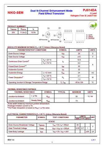
PJ614DA Dual N-Channel Enhancement Mode NIKO-SEM J-Lead Field Effect Transistor Halogen-Free & Lead-Free PRODUCT SUMMARY V(BR)DSS RDS(ON) ID 20V 11.8m 10.5A G GATE D DRAIN S SOURCE ABSOLUTE MAXIMUM RATINGS (TA = 25 C Unless Otherwise Noted) PARAMETERS/TEST CONDITIONS SYMBOL LIMITS UNITS Drain-Source Voltage VDS 20 V Gate-Source Voltage VGS 10 V TA = ... See More ⇒
Detailed specifications: PZ5203QV, PZ558EZ, PE6B0SA, PF610BC, PF610BL, PF610HV, PI506BZ, PI632BZ, 5N65, PC015BD, PC015HV, P2B60AMA, P2E03BK, P4004ED, P4006DV, P4402FAG, PD0903BEA
Keywords - PJ614DA MOSFET specs
PJ614DA cross reference
PJ614DA equivalent finder
PJ614DA pdf lookup
PJ614DA substitution
PJ614DA replacement
Can't find your MOSFET? Learn how to find a substitute transistor by analyzing voltage, current and package compatibility
