P6503FMA Datasheet. Specs and Replacement
Type Designator: P6503FMA 📄📄
Type of Transistor: MOSFET
Type of Control Channel: P-Channel
Absolute Maximum Ratings
Pd ⓘ - Maximum Power Dissipation: 0.96 W
|Vds|ⓘ - Maximum Drain-Source Voltage: 30 V
|Vgs|ⓘ - Maximum Gate-Source Voltage: 12 V
|Id| ⓘ - Maximum Drain Current: 3.1 A
Tj ⓘ - Maximum Junction Temperature: 150 °C
Electrical Characteristics
tr ⓘ - Rise Time: 100 nS
Cossⓘ - Output Capacitance: 79 pF
RDSonⓘ - Maximum Drain-Source On-State Resistance: 0.065 Ohm
Package: SOT23S
📄📄 Copy
P6503FMA substitution
- MOSFET ⓘ Cross-Reference Search
P6503FMA datasheet
p6503fma.pdf
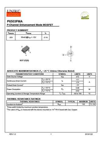
P6503FMA P-Channel Enhancement Mode MOSFET PRODUCT SUMMARY V(BR)DSS RDS(ON) ID 55m @VGS = -10V -30V -3.1A SOT-23(S) ABSOLUTE MAXIMUM RATINGS (TA = 25 C Unless Otherwise Noted) PARAMETERS/TEST CONDITIONS SYMBOL LIMITS UNITS VGS Gate-Source Voltage 12 V TA = 25 C -3.1 ID Continuous Drain Current TA = 70 A C -2.4 IDM -12 Pulsed Drain Current1 TA = 25 C 0.96... See More ⇒
p6503fm6.pdf
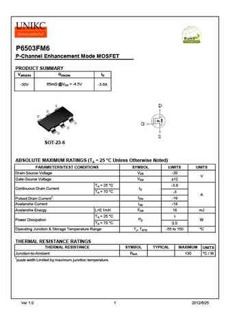
P6503FM6 P-Channel Enhancement Mode MOSFET PRODUCT SUMMARY V(BR)DSS RDS(ON) ID 65m @VGS = -4.5V -30V -3.6A SOT-23-6 ABSOLUTE MAXIMUM RATINGS (TA = 25 C Unless Otherwise Noted) PARAMETERS/TEST CONDITIONS SYMBOL LIMITS UNITS VDS Drain-Source Voltage -30 V VGS Gate-Source Voltage 12 TA = 25 C -3.6 ID Continuous Drain Current TA = 70 C -3 A IDM -19 Pulsed Drai... See More ⇒
p6503fm.pdf
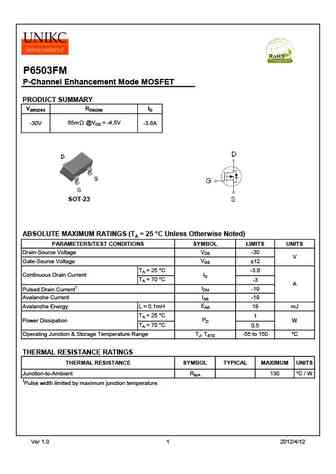
P6503FM P-Channel Enhancement Mode MOSFET PRODUCT SUMMARY V(BR)DSS RDS(ON) ID -30V 65m @VGS = -4.5V -3.6A SOT-23 ABSOLUTE MAXIMUM RATINGS (TA = 25 C Unless Otherwise Noted) PARAMETERS/TEST CONDITIONS SYMBOL LIMITS UNITS VDS Drain-Source Voltage -30 V VGS Gate-Source Voltage 12 TA = 25 C -3.6 ID Continuous Drain Current TA = 70 C -3 A IDM -19 Pulsed Drain C... See More ⇒
p6503nj.pdf
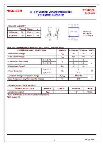
P6503NJ NIKO-SEM N- & P-Channel Enhancement Mode TSOPJW-8 Field Effect Transistor PRODUCT SUMMARY V(BR)DSS RDS(ON) ID G GATE 65m N-Channel 30 4A D DRAIN S SOURCE 150m -3A P-Channel -30 ABSOLUTE MAXIMUM RATINGS (TC = 25 C Unless Otherwise Noted) PARAMETERS/TEST CONDITIONS SYMBOL N-Channel P-Channel UNITS Drain-Source Voltage VDS 30 -30 V Gate-Source Vo... See More ⇒
Detailed specifications: P6015AT, P6015AV, P6015CDG, P6015CSG, P6402FMG, P6403FMG, P6503FM, P6503FM6, IRFP450, P6803HVG, PK610SA, PK612DZ, PK615BM6, PK615BMA, PK616BA, PK618BA, PK626BA
Keywords - P6503FMA MOSFET specs
P6503FMA cross reference
P6503FMA equivalent finder
P6503FMA pdf lookup
P6503FMA substitution
P6503FMA replacement
Step-by-step guide to finding a MOSFET replacement. Cross-reference parts and ensure compatibility for your repair or project.
