PK552DX Specs and Replacement
Type Designator: PK552DX
Type of Transistor: MOSFET
Type of Control Channel: N-Channel
Absolute Maximum Ratings
Pd ⓘ - Maximum Power Dissipation: 31 W
|Vds|ⓘ - Maximum Drain-Source Voltage: 20 V
|Vgs|ⓘ - Maximum Gate-Source Voltage: 8 V
|Id| ⓘ - Maximum Drain Current: 56 A
Tj ⓘ - Maximum Junction Temperature: 150 °C
Electrical Characteristics
tr ⓘ - Rise Time: 25 nS
Cossⓘ - Output Capacitance: 481 pF
RDSonⓘ - Maximum Drain-Source On-State Resistance: 0.0057 Ohm
Package: PDFN5X6P
PK552DX substitution
- MOSFET ⓘ Cross-Reference Search
PK552DX datasheet
pk552dx.pdf
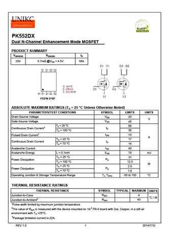
PK552DX Dual N-Channel Enhancement Mode MOSFET PRODUCT SUMMARY V(BR)DSS RDS(ON) ID 5.7m @VGS = 4.5V 20V 56A PDFN 5*6P ABSOLUTE MAXIMUM RATINGS (TA = 25 C Unless Otherwise Noted) PARAMETERS/TEST CONDITIONS SYMBOL LIMITS UNITS VDS Drain-Source Voltage 20 V VGS Gate-Source Voltage 8 TC = 25 C 56 ID Continuous Drain Current3 TC = 100 C 36 IDM 70 Pulsed Drain Cu... See More ⇒
pk552dx.pdf
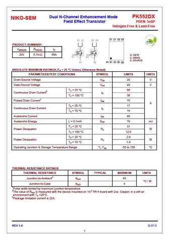
Dual N-Channel Enhancement Mode PK552DX NIKO-SEM Field Effect Transistor PDFN 5x6P Halogen-Free & Lead-Free D1 D1 D2 D2 D PRODUCT SUMMARY V(BR)DSS RDS(ON) ID G 20V 5.7m 56A G. GATE D. DRAIN S. SOURCE #1 S1 G1 S2 G2 S ABSOLUTE MAXIMUM RATINGS (TA = 25 C Unless Otherwise Noted) PARAMETERS/TEST CONDITIONS SYMBOL LIMITS UNITS Drain-Source Voltage VDS 20 V Gate... See More ⇒
Detailed specifications: PB210BM, PB210BTF, PB210BV, PB210HV, PK510BA, PK512BA, PK516BA, PK527BA, 2N7000, PK600BA, PK608BA, PK608DY, PB544DU, PB544JU, PB554DY, PB555BA, PB560DZ
Keywords - PK552DX MOSFET specs
PK552DX cross reference
PK552DX equivalent finder
PK552DX pdf lookup
PK552DX substitution
PK552DX replacement
Can't find your MOSFET? Learn how to find a substitute transistor by analyzing voltage, current and package compatibility
🌐 : EN ES РУ

LIST
Last Update
MOSFET: AUN084N10 | AUN065N10 | AUN063N10 | AUN062N08BG | AUN060N08AG | AUN053N10 | AUN050N08BGL | AUN045N085 | AUN042N055 | AUN036N10
Popular searches
c4468 datasheet | 2sc2603 | jcs50n20wt | 2sa1360 | p60nf06 datasheet | 2sc4468 | ru6888r | 2sc1815y