1115 Specs and Replacement
Type Designator: 1115
Type of Transistor: MOSFET
Type of Control Channel: N-Channel
Absolute Maximum Ratings
Pd ⓘ
- Maximum Power Dissipation: 330 W
|Vds|ⓘ - Maximum Drain-Source Voltage: 100 V
|Vgs|ⓘ - Maximum Gate-Source Voltage: 20 V
|Id| ⓘ - Maximum Drain Current: 150 A
Tj ⓘ - Maximum Junction Temperature: 175 °C
Electrical Characteristics
tr ⓘ - Rise Time: 100 nS
Cossⓘ -
Output Capacitance: 540 pF
RDSonⓘ - Maximum Drain-Source On-State Resistance: 0.0068 Ohm
Package: TO220
- MOSFET ⓘ Cross-Reference Search
1115 datasheet
..1. Size:2223K goford
1115.pdf 
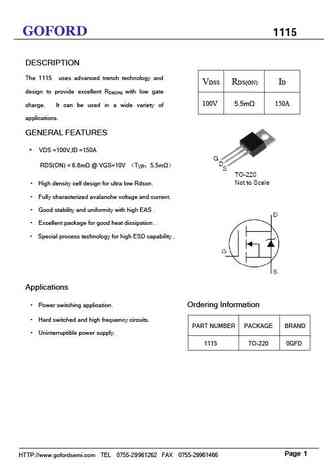
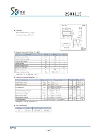
GOFORD 1115 DESCRIPTION The 1115 uses advanced trench technology and VDSS RDS(ON) ID design to provide excellent R with low gate DS(ON) 100V 5.5m 150A charge. It can be used in a wide variety of applications. GENERAL FEATURES VDS =100V,ID =150A RDS(ON) ... See More ⇒
0.1. Size:78K toshiba
2sk1115.pdf
Free Datasheet http //www.datasheet4u.com/ Free Datasheet http //www.datasheet4u.com/ ... See More ⇒
0.2. Size:174K toshiba
rn1114mfv rn1115mfv rn1116mfv rn1117mfv rn1118mfv.pdf
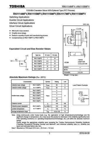
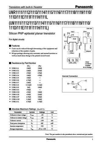
RN1114MFV RN1118MFV TOSHIBA Transistor Silicon NPN Epitaxial Type (PCT Process) RN1114MFV,RN1115MFV,RN1116MFV,RN1117MFV,RN1118MFV Switching Applications Inverter Circuit Applications Interface Circuit Applications Unit mm Driver Circuit Applications 1.2 0.05 With built-in bias resistors 0.80 0.05 Simplify circuit design Reduce a quantity of parts and manufac... See More ⇒
0.3. Size:111K renesas
rej03g1115 h5n5006ldlslmds.pdf
To our customers, Old Company Name in Catalogs and Other Documents On April 1st, 2010, NEC Electronics Corporation merged with Renesas Technology Corporation, and Renesas Electronics Corporation took over all the business of both companies. Therefore, although the old company name remains in this document, it is a valid Renesas Electronics document. We appreciate your understanding. ... See More ⇒
0.6. Size:80K ald
ald1115.pdf
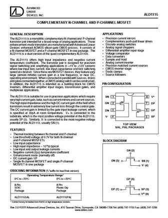
ADVANCED LINEAR ALD1115 DEVICES, INC. COMPLEMENTARY N-CHANNEL AND P-CHANNEL MOSFET APPLICATIONS GENERAL DESCRIPTION Precision current mirrors The ALD1115 is a monolithic complementary N-channel and P-channel Complementary push-pull linear drives transistor pair intended for a broad range of analog applications. These Discrete analog switches enhancement-mode transistors ... See More ⇒
0.8. Size:291K aosemi
aoss21115c.pdf
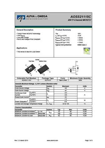
AOSS21115C 20V P-Channel MOSFET General Description Product Summary VDS Trench Power MOSFET technology -20V Low RDS(ON) ID (at VGS=-4.5V) -4.5A Low Gate Charge RDS(ON) (at VGS=-4.5V) ... See More ⇒
0.9. Size:611K aosemi
aots21115c.pdf
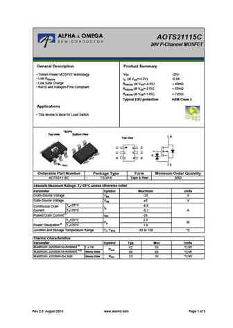
AOTS21115C 20V P-Channel MOSFET General Description Product Summary VDS Trench Power MOSFET technology -20V Low RDS(ON) ID (at VGS=-4.5V) -6.6A Low Gate Charge RDS(ON) (at VGS=-4.5V) ... See More ⇒
0.10. Size:367K aosemi
aote21115c.pdf

AOTE21115C 20V P-Channel MOSFET General Description Product Summary VDS Trench Power MOSFET technology -20V Low RDS(ON) ID (at VGS=-4.5V) -4.9A Low Gate Charge RDS(ON) (at VGS=-4.5V) ... See More ⇒
0.11. Size:1195K kexin
2sb1115.pdf
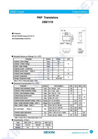
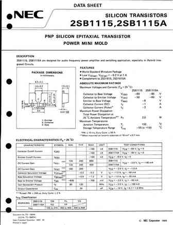
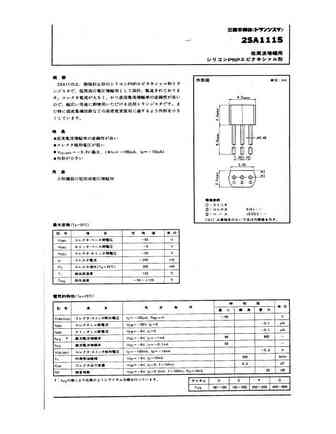
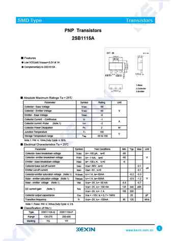
SMD Type Transistors PNP Transistors 2SB1115 Features 1.70 0.1 Low VCE(sat) VCE(sat)=-0.2V at 1A Complementary to 2SD1615 0.42 0.1 0.46 0.1 1.Base 2.Collector 3.Emitter Absolute Maximum Ratings Ta = 25 Parameter Symbol Rating Unit Collector - Base Voltage VCBO -60 Collector - Emitter Voltage VCEO -50 V Emitter - Base Voltage VEBO -6 Collector Current - ... See More ⇒
0.12. Size:1207K kexin
2sb1115a.pdf
SMD Type Transistors PNP Transistors 2SB1115A Features 1.70 0.1 Low VCE(sat) VCE(sat)=-0.2V at 1A Complementary to 2SD1615A 0.42 0.1 0.46 0.1 1.Base 2.Collector 3.Emitter Absolute Maximum Ratings Ta = 25 Parameter Symbol Rating Unit Collector - Base Voltage VCBO -80 Collector - Emitter Voltage VCEO -60 V Emitter - Base Voltage VEBO -6 Collector Current ... See More ⇒
0.14. Size:176K inchange semiconductor
2sc1115.pdf
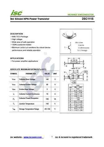
INCHANGE Semiconductor isc Silicon NPN Power Transistor 2SC1115 DESCRIPTION With TO-3 Package High voltage Wide area of safe operation 100% avalanche tested Minimum Lot-to-Lot variations for robust device performance and reliable operation APPLICATIONS For power amplifier applications ABSOLUTE MAXIMUM RATINGS(T =25 ) a SYMBOL PARAMETER VALUE UNIT V Collector-Base Vol... See More ⇒
0.15. Size:209K inchange semiconductor
2sd1115.pdf
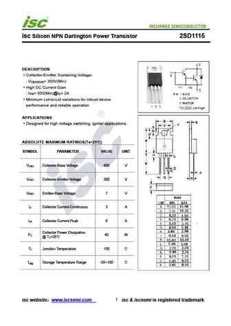
isc Silicon NPN Darlington Power Transistor 2SD1115 DESCRIPTION Collector-Emitter Sustaining Voltage- V = 300V(Min) CEO(SUS) High DC Current Gain h = 500(Min)@I = 2A FE C Minimum Lot-to-Lot variations for robust device performance and reliable operation APPLICATIONS Designed for high voltage switching, igniter applications. ABSOLUTE MAXIMUM RATINGS(T =25 ) a SYMBOL P... See More ⇒
0.16. Size:260K inchange semiconductor
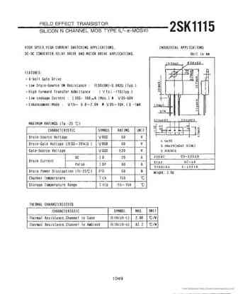
2sk1115.pdf
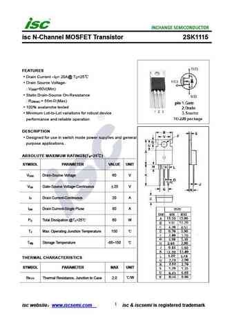
isc N-Channel MOSFET Transistor 2SK1115 FEATURES Drain Current I = 20A@ T =25 D C Drain Source Voltage- V =60V(Min) DSS Static Drain-Source On-Resistance R = 55m (Max) DS(on) 100% avalanche tested Minimum Lot-to-Lot variations for robust device performance and reliable operation DESCRIPTION Designed for use in switch mode power supplies and general purpose ... See More ⇒
0.17. Size:57K inchange semiconductor
2sd1115k.pdf
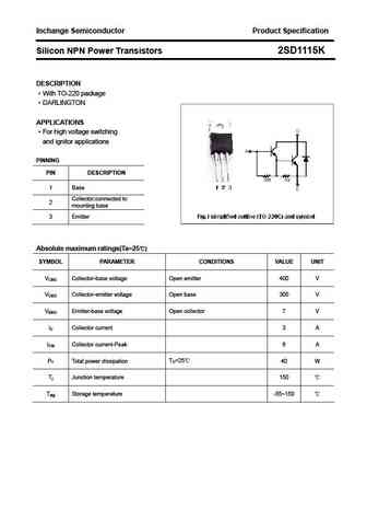
Inchange Semiconductor Product Specification Silicon NPN Power Transistors 2SD1115K DESCRIPTION With TO-220 package DARLINGTON APPLICATIONS For high voltage switching and ignitor applications PINNING PIN DESCRIPTION 1 Base Collector;connected to 2 mounting base 3 Emitter Absolute maximum ratings(Ta=25 ) SYMBOL PARAMETER CONDITIONS VALUE UNIT VCBO Collecto... See More ⇒
Detailed specifications: SSS10N60
, SSS12N60
, SSS1N60
, SSS2N60
, SSS5N60
, SSS7N60
, SSS8N60
, 1002
, AON7403
, 1515
, G1601
, 2300
, 2301
, 2302
, 3035
, 3400
, 3401
.
Keywords - 1115 MOSFET specs
1115 cross reference
1115 equivalent finder
1115 pdf lookup
1115 substitution
1115 replacement
Need a MOSFET replacement?
Our guide shows you how to find a perfect substitute by comparing key parameters and specs