25P06 Datasheet. Specs and Replacement
Type Designator: 25P06 📄📄
Type of Transistor: MOSFET
Type of Control Channel: P-Channel
Absolute Maximum Ratings
Pd ⓘ - Maximum Power Dissipation: 90 W
|Vds|ⓘ - Maximum Drain-Source Voltage: 60 V
|Vgs|ⓘ - Maximum Gate-Source Voltage: 20 V
|Id| ⓘ - Maximum Drain Current: 25 A
Tj ⓘ - Maximum Junction Temperature: 150 °C
Electrical Characteristics
tr ⓘ - Rise Time: 15 nS
Cossⓘ - Output Capacitance: 391 pF
RDSonⓘ - Maximum Drain-Source On-State Resistance: 0.045 Ohm
Package: TO220
📄📄 Copy
- MOSFET ⓘ Cross-Reference Search
25P06 datasheet
..1. Size:1738K goford
25p06.pdf 
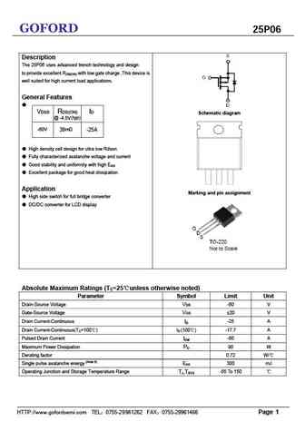
GOFORD 25P06 Description The 25P06 uses advanced trench technology and design to provide excellent RDS(ON) with low gate charge .This device is well suited for high current load applications. General Features VDSS RDS(ON) ID Schematic diagram @ -4.5V (typ) -60V m -25A 39 High density cell design for ultra low Rdson Fully characterized avalanche voltage an... See More ⇒
0.1. Size:829K 1
hm25p06d.pdf

HM25P06D P-Channel Enhancement Mode Power MOSFET Description The HM25P06D uses advanced trench technology and design to provide excellent RDS(ON) with low gate charge .This device is well suited for high current load applications. General Features VDS =-60V,ID =-25A RDS(ON) ... See More ⇒
0.2. Size:67K onsemi
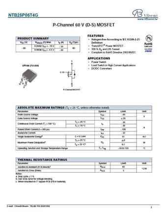
ntb25p06-d.pdf
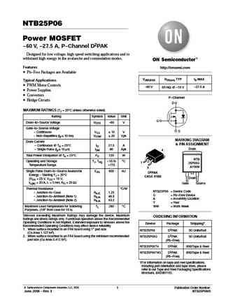
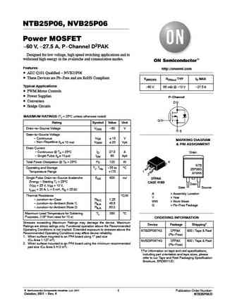
NTB25P06 Power MOSFET -60 V, -27.5 A, P-Channel D2PAK Designed for low voltage, high speed switching applications and to withstand high energy in the avalanche and commutation modes. Features http //onsemi.com Pb-Free Packages are Available V(BR)DSS RDS(on) TYP ID MAX Typical Applications PWM Motor Controls -60 V 65 mW @ -10 V -27.5 A Power Supplies Converters P-Ch... See More ⇒
0.5. Size:150K utc
utt25p06.pdf
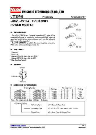
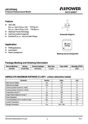
UNISONIC TECHNOLOGIES CO., LTD UTT25P06 Preliminary Power MOSFET -60V, -27.5A P-CHANNEL POWER MOSFET DESCRIPTION The UTC UTT25P06 is a P-channel power MOSFET using UTC s advanced technology to provide the customers with high switching speed and a minimum on-state resistance, and it can also withstand high energy in the avalanche. This UTC UTT25P06 is suitable for power sup... See More ⇒
0.6. Size:339K cystek
mtb25p06fp.pdf
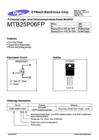
Spec. No. C584FP Issued Date 2014.07.03 CYStech Electronics Corp. Revised Date Page No. 1/8 P-Channel Logic Level Enhancement Mode Power MOSFET BVDSS -60V MTB25P06FP ID -52A RDS(ON)@VGS=-10V, ID=-20A 18.8m (typ) RDS(ON)@VGS=-4.5V, ID=-20A 21.8m (typ) Features Low Gate Charge Simple Drive Requirement Pb-free lead plating package Equivalent Circu... See More ⇒
0.7. Size:590K way-on
wmq25p06ts.pdf
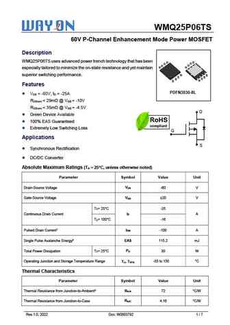
WMQ25P06TS 60V P-Channel Enhancement Mode Power MOSFET Description WMQ25P06TS uses advanced power trench technology that has been D D D D D D D D especially tailored to minimize the on-state resistance and yet maintain superior switching performance. G ss s ss G s Features PDFN3030-8L V = -60V, I = -25A DS D R ... See More ⇒
0.8. Size:610K way-on
wmo25p06t1.pdf
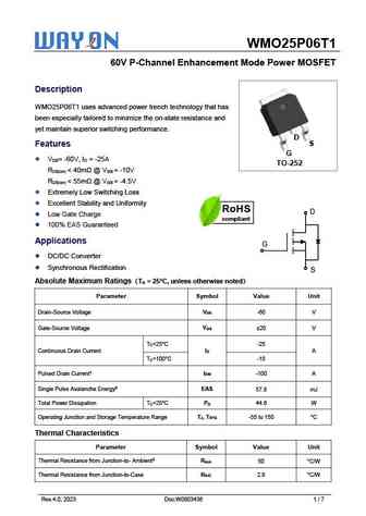
WMO25P06T1 60V P-Channel Enhancement Mode Power MOSFET Description WMO25P06T1 uses advanced power trench technology that has been especially tailored to minimize the on-state resistance and yet maintain superior switching performance. D S Features G V = -60V, I = -25A DS D TO-252 R ... See More ⇒
0.11. Size:1447K cn vbsemi
ntb25p06t4g.pdf
NTB25P06T4G www.VBsemi.tw P-Channel 60 V (D-S) MOSFET FEATURES PRODUCT SUMMARY Halogen-free According to IEC 61249-2-21 VDS (V) RDS(on) ( ) Max. ID (A) Qg (Typ.) Definition TrenchFET Power MOSFET 0.048at VGS = - 10 V - 35 - 60 60 100 % Rg and UIS Tested 0.060at VGS = - 4.5 V - 30 Compliant to RoHS Directive 2002/95/EC APPLICATIONS S Power Switch Lo... See More ⇒
0.12. Size:883K cn vbsemi
hm25p06k.pdf
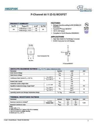
HM25P06K www.VBsemi.tw P-Channel 60 V (D-S) MOSFET FEATURES PRODUCT SUMMARY Halogen-free According to IEC 61249-2-21 VDS (V) RDS(on) ( ) ID (A)d Qg (Typ) Definition 0.053 at VGS = - 10 V - 25 TrenchFET Power MOSFET - 60 26 0.062 at VGS = - 4.5 V - 20 100 % UIS Tested Compliant to RoHS Directive 2002/95/EC APPLICATIONS High Side Switch for Full Bridge Con... See More ⇒
0.13. Size:829K cn hmsemi
hm25p06d.pdf
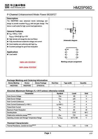
HM25P06D P-Channel Enhancement Mode Power MOSFET Description The HM25P06D uses advanced trench technology and design to provide excellent RDS(ON) with low gate charge .This device is well suited for high current load applications. General Features VDS =-60V,ID =-25A RDS(ON) ... See More ⇒
0.14. Size:1028K cn hmsemi
hm25p06k.pdf
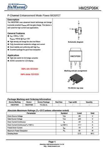
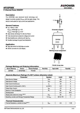
HM25P06K P-Channel Enhancement Mode Power MOSFET Description The HM25P06K uses advanced trench technology and design to provide excellent RDS(ON) with low gate charge .This device is well suited for high current load applications. General Features VDS =-60V,ID =-25A RDS(ON) ... See More ⇒
Detailed specifications: 16N10, 18N10, 2002A, 20P10, 21N06, 22N10, 2301H, 2301L, K4145, 25P10, 25P10G, 28N10, 28P55, 30P10A, 30P55, 3205PL, 3205TR
Keywords - 25P06 MOSFET specs
25P06 cross reference
25P06 equivalent finder
25P06 pdf lookup
25P06 substitution
25P06 replacement
Step-by-step guide to finding a MOSFET replacement. Cross-reference parts and ensure compatibility for your repair or project.