G1010 Specs and Replacement
Type Designator: G1010
Type of Transistor: MOSFET
Type of Control Channel: N-Channel
Absolute Maximum Ratings
Pd ⓘ - Maximum Power Dissipation: 200 W
|Vds|ⓘ - Maximum Drain-Source Voltage: 60 V
|Vgs|ⓘ - Maximum Gate-Source Voltage: 20 V
|Id| ⓘ - Maximum Drain Current: 100 A
Tj ⓘ - Maximum Junction Temperature: 175 °C
Electrical Characteristics
tr ⓘ - Rise Time: 50.8 nS
Cossⓘ - Output Capacitance: 671.5 pF
RDSonⓘ - Maximum Drain-Source On-State Resistance: 0.01 Ohm
Package: TO220
G1010 substitution
- MOSFET ⓘ Cross-Reference Search
G1010 datasheet
g1010.pdf
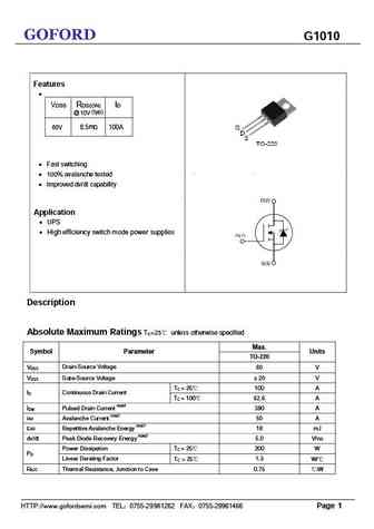
GOFORD G1010 Features VDSS RDS(ON) ID @ 10V (typ) 8.5m 100A 60V Fast switching 100% avalanche tested Improved dv/dt capability Application UPS High efficiency switch mode power supplies Description Absolute Maximum Ratings TC=25 unless otherwise specified Max. Symbol Parameter Units TO-220 V Drain-Source Voltage 60 V DSS V Gate... See More ⇒
rej03g1010 2sk2393ds.pdf
To our customers, Old Company Name in Catalogs and Other Documents On April 1st, 2010, NEC Electronics Corporation merged with Renesas Technology Corporation, and Renesas Electronics Corporation took over all the business of both companies. Therefore, although the old company name remains in this document, it is a valid Renesas Electronics document. We appreciate your understanding. ... See More ⇒
pg1010bk.pdf
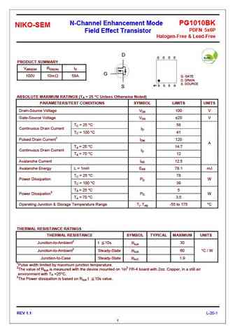
N-Channel Enhancement Mode PG1010BK NIKO-SEM PDFN 5x6P Field Effect Transistor Halogen-Free & Lead-Free D D D D D PRODUCT SUMMARY V(BR)DSS RDS(ON) ID G 100V 10m 58A G. GATE D. DRAIN S. SOURCE #1 S S S G S ABSOLUTE MAXIMUM RATINGS (TA = 25 C Unless Otherwise Noted) PARAMETERS/TEST CONDITIONS SYMBOL LIMITS UNITS Drain-Source Voltage VDS 100 V Gate-Source Vol... See More ⇒
pg1010bd.pdf
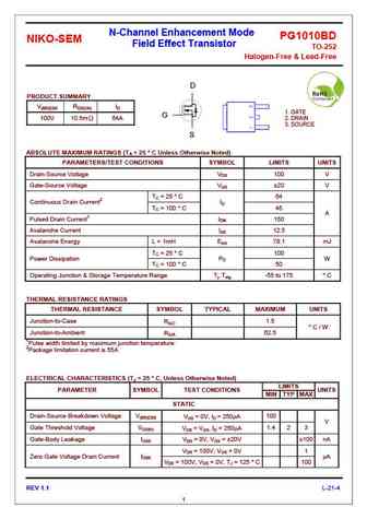
N-Channel Enhancement Mode PG1010BD NIKO-SEM Field Effect Transistor TO-252 Halogen-Free & Lead-Free D PRODUCT SUMMARY V(BR)DSS RDS(ON) ID 1. GATE G 100V 10.5m 64A 2. DRAIN 3. SOURCE S ABSOLUTE MAXIMUM RATINGS (TA = 25 C Unless Otherwise Noted) PARAMETERS/TEST CONDITIONS SYMBOL LIMITS UNITS Drain-Source Voltage VDS 100 V Gate-Source Voltage VGS 20 V TC =... See More ⇒
Detailed specifications: 6706A, 68P40, 80N03, 80N04, 80N08TR, 8205A, 8205B, G3205, IRFP064N, G3710, 5N20A, 630A, 640, 18N20, 18N20A, 2N25, 3N25
Keywords - G1010 MOSFET specs
G1010 cross reference
G1010 equivalent finder
G1010 pdf lookup
G1010 substitution
G1010 replacement
Need a MOSFET replacement? Our guide shows you how to find a perfect substitute by comparing key parameters and specs
History: SFW132N200I3 | G3710 | SLC500MM20SHN2
🌐 : EN ES РУ

LIST
Last Update
MOSFET: ASU70R600E | ASU65R850E | ASU65R550E | ASU65R350E | ASR65R120EFD | ASR65R046EFD | ASQ65R046EFD | ASM65R280E | ASM60R330E | ASE70R950E
Popular searches
g40t60an3h datasheet | j5027-r datasheet | transistor a1015 datasheet | bf199 transistor equivalent | bu801 | c8550 transistor datasheet | mj21194 transistor datasheet | kep40n26