IXTA15N50L2 Specs and Replacement
Type Designator: IXTA15N50L2
Type of Transistor: MOSFET
Type of Control Channel: N-Channel
Absolute Maximum Ratings
Pd ⓘ - Maximum Power Dissipation: 300 W
|Vds|ⓘ - Maximum Drain-Source Voltage: 500 V
|Vgs|ⓘ - Maximum Gate-Source Voltage: 20 V
|Id| ⓘ - Maximum Drain Current: 15 A
Tj ⓘ - Maximum Junction Temperature: 150 °C
Electrical Characteristics
tr ⓘ - Rise Time: 73 nS
Cossⓘ - Output Capacitance: 265 pF
Rds ⓘ - Maximum Drain-Source On-State Resistance: 0.48 Ohm
Package: TO-263AA
IXTA15N50L2 substitution
- MOSFET ⓘ Cross-Reference Search
IXTA15N50L2 datasheet
ixta15n50l2.pdf
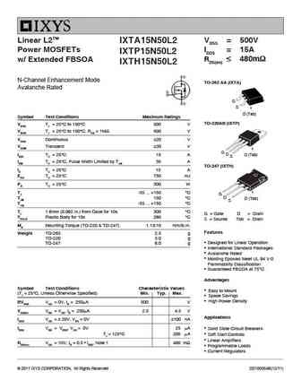
Linear L2TM VDSS = 500V IXTA15N50L2 Power MOSFETs ID25 = 15A IXTP15N50L2 RDS(on) 480m w/ Extended FBSOA IXTH15N50L2 N-Channel Enhancement Mode TO-263 AA (IXTA) Avalanche Rated G S D (Tab) Symbol Test Conditions Maximum Ratings TO-220AB (IXTP) VDSS TJ = 25 C to 150 C 500 V VDGR TJ = 25 C to 150 C, RGS = 1M 500 V VGSS Continuous 20 V ... See More ⇒
ixta152n085t ixtp152n085t.pdf
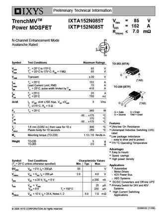
Preliminary Technical Information VDSS = 85 V IXTA152N085T TrenchMVTM ID25 = 152 A IXTP152N085T Power MOSFET RDS(on) 7.0 m N-Channel Enhancement Mode Avalanche Rated Symbol Test Conditions Maximum Ratings TO-263 (IXTA) VDSS TJ = 25 C to 175 C85 V VDGR TJ = 25 C to 175 C; RGS = 1 M 85 V G VGSM Transient 20 V S (TAB) ID25 ... See More ⇒
ixta152n085t7.pdf
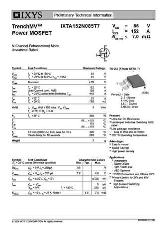
Preliminary Technical Information VDSS = 85 V IXTA152N085T7 TrenchMVTM ID25 = 152 A Power MOSFET RDS(on) 7.0 m N-Channel Enhancement Mode Avalanche Rated Symbol Test Conditions Maximum Ratings TO-263 (7-lead) (IXTA..7) VDSS TJ = 25 C to 175 C85 V VDGR TJ = 25 C to 175 C; RGS = 1 M 85 V VGSM Transient 20 V 1 ID25 TC = 25 ... See More ⇒
ixta152n085t.pdf
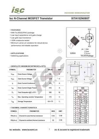
Isc N-Channel MOSFET Transistor IXTA152N085T FEATURES With To-263(D2PAK) package Low input capacitance and gate charge Low gate input resistance 100% avalanche tested Minimum Lot-to-Lot variations for robust device performance and reliable operation APPLICATIONS Switching applications ABSOLUTE MAXIMUM RATINGS(T =25 ) a SYMBOL PARAMETER VALUE UNIT V Drain-Source ... See More ⇒
Detailed specifications: IXTA3N120TRL , IXTA3N120HV , IXTA3N100D2HV , IXTA270N04T4 , IXTA20N65X , IXTA1N200P3HV , IXTA1N170DHV , IXTA180N055T , IRFB3607 , IXTA130N10T-TRL , IXTA12N65X2 , IXTA08N100D2HV , IXTA05N100HV , IXTA02N450HV , IXTA02N250HV , IXTA02N250 , IXKP35N60C5 .
History: BL5N50-D
Keywords - IXTA15N50L2 MOSFET specs
IXTA15N50L2 cross reference
IXTA15N50L2 equivalent finder
IXTA15N50L2 pdf lookup
IXTA15N50L2 substitution
IXTA15N50L2 replacement
Learn how to find the right MOSFET substitute. A guide to cross-reference, check specs and replace MOSFETs in your circuits.
History: BL5N50-D


LIST
Last Update
MOSFET: AOTF20N40L | AOTF11N60L | AOT11N60L | AONS21303C | AOI280A60 | AOB66914L | AO3485C | AOI780A70 | AOB42S60L | AOTF950A70L
Popular searches
2n3903 transistor | 2n4360 | 2n2613 | c2166 transistor | 2sd330 | 20n60 | ksa1013 | mje15032g datasheet