FDFMA3N109 Specs and Replacement
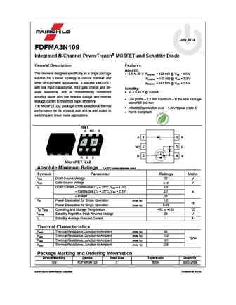
Type Designator: FDFMA3N109
Type of Transistor: MOSFET
Type of Control Channel: N-Channel
Absolute Maximum Ratings
Pd ⓘ - Maximum Power Dissipation: 1.5 W
|Vds|ⓘ - Maximum Drain-Source Voltage: 30 V
|Vgs|ⓘ - Maximum Gate-Source Voltage: 12 V
|Id| ⓘ - Maximum Drain Current: 2.9 A
Tj ⓘ - Maximum Junction Temperature: 150 °C
Electrical Characteristics
tr ⓘ - Rise Time: 8 nS
Cossⓘ - Output Capacitance: 30 pF
RDSonⓘ - Maximum Drain-Source On-State Resistance: 0.123 Ohm
Package: MICROFET2X2
FDFMA3N109 substitution
- MOSFET ⓘ Cross-Reference Search
FDFMA3N109 datasheet
fdfma3n109.pdf
July 2014 FDFMA3N109 Integrated N-Channel PowerTrench MOSFET and Schottky Diode General Description Features MOSFET This device is designed specifically as a single package 2.9 A, 30 V RDS(ON) = 123 m @ VGS = 4.5 V solution for a boost topology in cellular handset and RDS(ON) = 140 m @ VGS = 3.0 V other ultra-portable applications. It features a MOSFET = 163 m ... See More ⇒
fdfma2p857.pdf
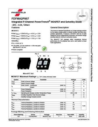
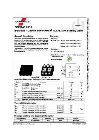
July 2014 FDFMA2P857 Integrated P-Channel PowerTrench MOSFET and Schottky Diode 20V, 3.0A, 120m Features General Description This device is designed specifically as a single package solution MOSFET for the battery charge switch in cellular handset and other ultra- Max rDS(on) = 120m at VGS = 4.5V, ID = 3.0A portable applications. It features a MOSFET with low on-s... See More ⇒
fdfma2p853t.pdf
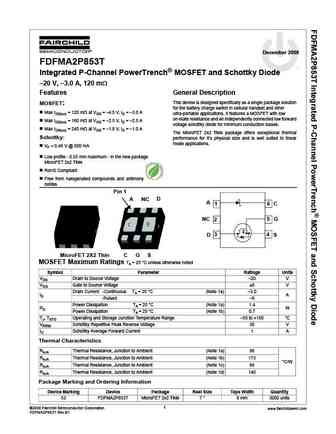
December 2008 FDFMA2P853T tm Integrated P-Channel PowerTrench MOSFET and Schottky Diode 20 V, 3.0 A, 120 m Features General Description This device is designed specifically as a single package solution MOSFET for the battery charge switch in cellular handset and other Max rDS(on) = 120 m at VGS = 4.5 V, ID = 3.0 A ultra-portable applications. It features a MOS... See More ⇒
fdfma2p029z.pdf
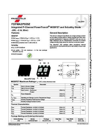
July 2014 FDFMA2P029Z Integrated P-Channel PowerTrench MOSFET and Schottky Diode 20V, 3.1A, 95m Features General Description MOSFET This device is designed specifically as a single package solution for the battery charge switch in cellular handset and other ultra- Max rDS(on) = 95m at VGS = 4.5V, ID = 3.1A portable applications. It features a MOSFET with very low on- ... See More ⇒
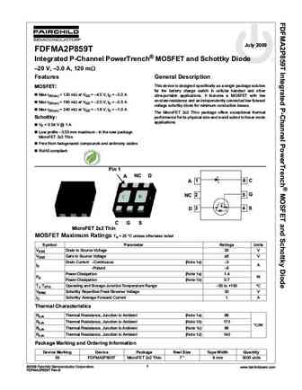
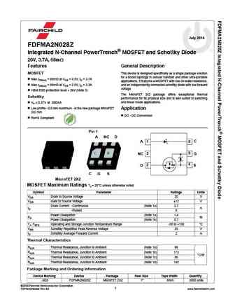
Detailed specifications: FDFM2N111, FDFM2P110, FDFMA2N028Z, FDFMA2P029Z, FDFMA2P853, FDFMA2P853T, FDFMA2P857, FDFMA2P859T, IRF1010E, FDFME2P823ZT, FDFME3N311ZT, FDFMJ2P023Z, FDFS2P102, FDFS2P102A, FDFS2P103, FDFS2P103A, FDFS2P106A
Keywords - FDFMA3N109 MOSFET specs
FDFMA3N109 cross reference
FDFMA3N109 equivalent finder
FDFMA3N109 pdf lookup
FDFMA3N109 substitution
FDFMA3N109 replacement
Step-by-step guide to finding a MOSFET replacement. Cross-reference parts and ensure compatibility for your repair or project.
🌐 : EN ES РУ
LIST
Last Update
MOSFET: CM4407 | CM3407 | CM3400 | SVF11N65F | SVF11N65T | FKBB3105 | EHBA036R1 | CRTT067N10N | AP6NA3R2MT | AP65SA145DDT8
Popular searches
irfb4110 | tip36c | bd139 transistor | irf840 datasheet | ge10001 | irf830 | irfp450 | mj21193
