FDV301NNB9V005 Specs and Replacement
Type Designator: FDV301NNB9V005
Type of Transistor: MOSFET
Type of Control Channel: N-Channel
Absolute Maximum Ratings
Pd ⓘ - Maximum Power Dissipation: 0.35 W
|Vds|ⓘ - Maximum Drain-Source Voltage: 25 V
|Vgs|ⓘ - Maximum Gate-Source Voltage: 8 V
|Id| ⓘ - Maximum Drain Current: 0.22 A
Tj ⓘ - Maximum Junction Temperature: 150 °C
Electrical Characteristics
tr ⓘ - Rise Time: 6 nS
Cossⓘ - Output Capacitance: 6 pF
RDSonⓘ - Maximum Drain-Source On-State Resistance: 4 Ohm
Package: SOT-23
FDV301NNB9V005 substitution
- MOSFET ⓘ Cross-Reference Search
FDV301NNB9V005 datasheet
fdv301n d87z fdv301n nb9v005.pdf
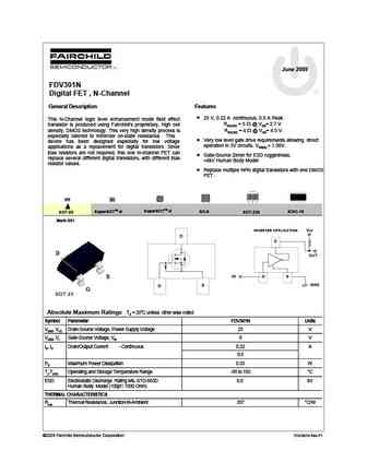
June 2009 FDV301N Digital FET , N-Channel General Description Features 25 V, 0.22 A continuous, 0.5 A Peak. This N-Channel logic level enhancement mode field effect RDS(ON) = 5 @ VGS= 2.7 V transistor is produced using Fairchild's proprietary, high cell density, DMOS technology. This very high density process is RDS(ON) = 4 @ VGS= 4.5 V. especially tailored to minimize on-... See More ⇒
fdv301n.pdf
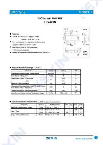
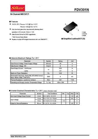
N-Channel MOSFET FDV301N SOT-23 Unit mm +0.1 2.9 -0.1 +0.1 0.4 -0.1 3 1 2 +0.1 +0.05 0.95-0.1 0.1-0.01 +0.1 1.9-0.1 1. Gate 2. Source 3. Drain 0.4 +0.1 +0.1 2.4 -0.1 1.3 -0.1 0.55 +0.1 0.97 -0.1 +0.1 0-0.1 0.38 -0.1 N-Channel MOSFET FDV301N Marking Marking 301 SMD Type MOSFET N-Channel MOSFET FDV301N Typical Characterisitics 1.4 0.5 V GS = 4... See More ⇒
Detailed specifications: FDU8870, FDU8874, FDU8876, FDU8878, FDU8880, FDU8882, FDU8896, FDV301ND87Z, 2SK3568, FDV302PD87Z, FDV302PNB8V001, FDV303NNB9U008, FDV304PD87Z, FDV304PNB8U003, FDW252P, FDW254P, FDW254PZ
Keywords - FDV301NNB9V005 MOSFET specs
FDV301NNB9V005 cross reference
FDV301NNB9V005 equivalent finder
FDV301NNB9V005 pdf lookup
FDV301NNB9V005 substitution
FDV301NNB9V005 replacement
Can't find your MOSFET? Learn how to find a substitute transistor by analyzing voltage, current and package compatibility
🌐 : EN ES РУ
LIST
Last Update
MOSFET: AUW033N08BG | AUW025N10 | AUR030N10 | AUR020N10 | AUR020N085 | AUR014N10 | AUP074N10 | AUP065N10 | AUP062N08BG | AUP060N08AG
Popular searches
bd243 | 2sk170 datasheet | 2n7000 equivalent | tip31 | tip122 transistor | 2sc1079 | 2sc1815 equivalent | 2sa1220


