SSF3612E Datasheet. Specs and Replacement
Type Designator: SSF3612E 📄📄
Type of Transistor: MOSFET
Type of Control Channel: N-Channel
Absolute Maximum Ratings
Pd ⓘ - Maximum Power Dissipation: 3.1 W
|Vds|ⓘ - Maximum Drain-Source Voltage: 25 V
|Vgs|ⓘ - Maximum Gate-Source Voltage: 12 V
|Id| ⓘ - Maximum Drain Current: 11 A
Tj ⓘ - Maximum Junction Temperature: 150 °C
Electrical Characteristics
tr ⓘ - Rise Time: 4.42 nS
Cossⓘ - Output Capacitance: 291 pF
RDSonⓘ - Maximum Drain-Source On-State Resistance: 0.012 Ohm
Package: SOP-8
SSF3612E substitution
- MOSFET ⓘ Cross-Reference Search
SSF3612E datasheet
ssf3612e.pdf
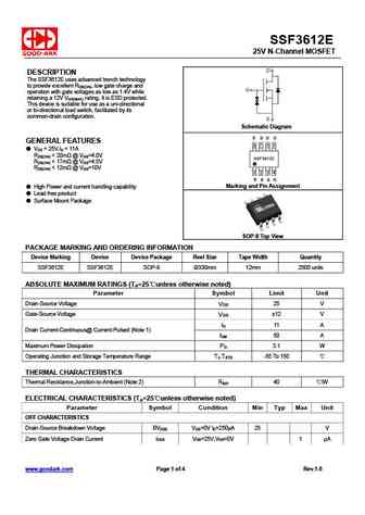
SSF3612E 25V N-Channel MOSFET DESCRIPTION The SSF3612E uses advanced trench technology to provide excellent RDS(ON), low gate charge and operation with gate voltages as low as 1.4V while retaining a 12V VGS(MAX) rating. It is ESD protected. This device is suitable for use as a uni-directional or bi-directional load switch, facilitated by its common-drain configuration. Schem... See More ⇒
ssf3612.pdf
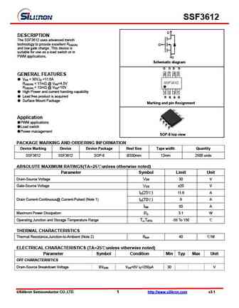
SSF3612 D DESCRIPTION The SSF3612 uses advanced trench technology to provide excellent RDS(ON) G and low gate charge .This device is suitable for use as a load switch or in PWM applications. S Schematic diagram GENERAL FEATURES VDS = 30V,ID =11.6A RDS(ON) ... See More ⇒
ssf3616.pdf

SSF3616 D DESCRIPTION The SSF3616 uses advanced trench technology to provide excellent RDS(ON) G and low gate charge .This device is suitable for use as a load switch or in PWM applications. S Schematic diagram GENERAL FEATURES VDS = 30V,ID =9A RDS(ON) ... See More ⇒
ssf3617.pdf
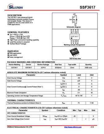
SSF3617 D DESCRIPTION The SSF3617 uses advanced trench technology to provide excellent RDS(ON) G and low gate charge .This device is suitable for use as a load switch or in PWM applications. S Schematic diagram GENERAL FEATURES VDS =-30V,ID =-10A RDS(ON) ... See More ⇒


Detailed specifications: SQR50N06-07L, SSF22A5E, SSF2418B, SSF2418EBK, SSF2439E, SSF2641S, SSF2816EBK, SSF2N60D1, 75N75, R9523, SSF440M, SSF450M, SSF5508D, SSF5510G, SSF6010G, SSF7008, TJ100F04M3L
Keywords - SSF3612E MOSFET specs
SSF3612E cross reference
SSF3612E equivalent finder
SSF3612E pdf lookup
SSF3612E substitution
SSF3612E replacement
Need a MOSFET replacement? Our guide shows you how to find a perfect substitute by comparing key parameters and specs
History: SFG170N10PF
🌐 : EN ES РУ

LIST
Last Update
MOSFET: ASDM30P100KQ | ASDM30N90Q | ASDM30N75KQ | ASDM30N150Q | ASDM30N120Q | ASDM30N120KQ | ASDM30N100KQ | ASDM30DN40E | ASDM30DN30E | ASDM3050KQ
Popular searches
a1046 transistor | hy19p03 | 2sk2749 | c2577 transistor | k3563 transistor | 2sc1775 datasheet | j377 transistor datasheet | svt20240nt