SSF3612E datasheet, аналоги, основные параметры
Наименование производителя: SSF3612E 📄📄
Тип транзистора: MOSFET
Полярность: N
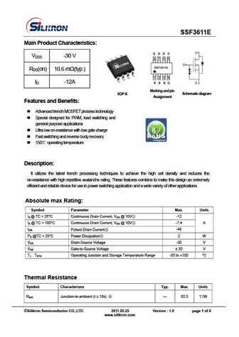
Предельные значения
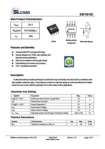
Pd ⓘ - Максимальная рассеиваемая мощность: 3.1 W
|Vds|ⓘ - Максимально допустимое напряжение сток-исток: 25 V
|Vgs|ⓘ - Максимально допустимое напряжение затвор-исток: 12 V
|Id| ⓘ - Максимально допустимый постоянный ток стока: 11 A
Tj ⓘ - Максимальная температура канала: 150 °C
Электрические характеристики
tr ⓘ - Время нарастания: 4.42 ns
Cossⓘ - Выходная емкость: 291 pf
RDSonⓘ - Сопротивление сток-исток открытого транзистора: 0.012 Ohm
Тип корпуса: SOP-8
📄📄 Копировать ⓘ
Аналог (замена) для SSF3612E
- подборⓘ MOSFET транзистора по параметрам
SSF3612E даташит
ssf3612e.pdf
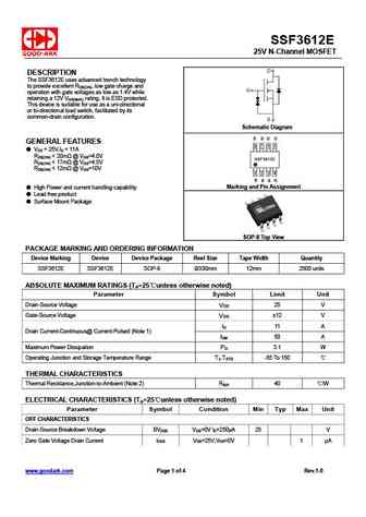
SSF3612E 25V N-Channel MOSFET DESCRIPTION The SSF3612E uses advanced trench technology to provide excellent RDS(ON), low gate charge and operation with gate voltages as low as 1.4V while retaining a 12V VGS(MAX) rating. It is ESD protected. This device is suitable for use as a uni-directional or bi-directional load switch, facilitated by its common-drain configuration. Schem
ssf3612.pdf
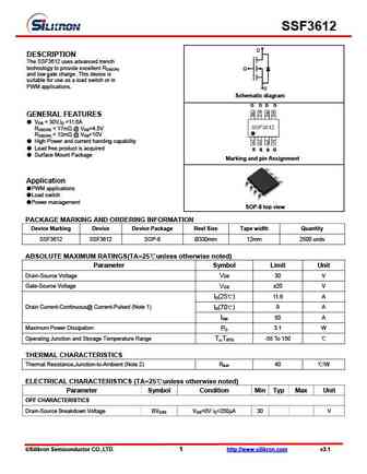
SSF3612 D DESCRIPTION The SSF3612 uses advanced trench technology to provide excellent RDS(ON) G and low gate charge .This device is suitable for use as a load switch or in PWM applications. S Schematic diagram GENERAL FEATURES VDS = 30V,ID =11.6A RDS(ON)
ssf3616.pdf

SSF3616 D DESCRIPTION The SSF3616 uses advanced trench technology to provide excellent RDS(ON) G and low gate charge .This device is suitable for use as a load switch or in PWM applications. S Schematic diagram GENERAL FEATURES VDS = 30V,ID =9A RDS(ON)
ssf3617.pdf
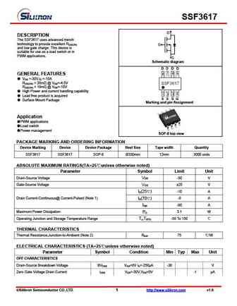
SSF3617 D DESCRIPTION The SSF3617 uses advanced trench technology to provide excellent RDS(ON) G and low gate charge .This device is suitable for use as a load switch or in PWM applications. S Schematic diagram GENERAL FEATURES VDS =-30V,ID =-10A RDS(ON)


Другие IGBT... SQR50N06-07L, SSF22A5E, SSF2418B, SSF2418EBK, SSF2439E, SSF2641S, SSF2816EBK, SSF2N60D1, 75N75, R9523, SSF440M, SSF450M, SSF5508D, SSF5510G, SSF6010G, SSF7008, TJ100F04M3L
🌐 : EN ES РУ

Список транзисторов
Обновления
MOSFET: ASDM30P100KQ | ASDM30N90Q | ASDM30N75KQ | ASDM30N150Q | ASDM30N120Q | ASDM30N120KQ | ASDM30N100KQ | ASDM30DN40E | ASDM30DN30E | ASDM3050KQ | ASDM2305 | ASDM2301 | ASDM2300ZA | ASDM20P13S | ASDM20N90Q | ASDM20N60
Popular searches
a1046 transistor | hy19p03 | 2sk2749 | c2577 transistor | k3563 transistor | 2sc1775 datasheet | j377 transistor datasheet | svt20240nt