IRFW510A Specs and Replacement
Type Designator: IRFW510A
Type of Transistor: MOSFET
Type of Control Channel: N-Channel
Absolute Maximum Ratings
Pd ⓘ
- Maximum Power Dissipation: 33 W
|Vds|ⓘ - Maximum Drain-Source Voltage: 100 V
|Vgs|ⓘ - Maximum Gate-Source Voltage: 20 V
|Id| ⓘ - Maximum Drain Current: 5.6 A
Tj ⓘ - Maximum Junction Temperature: 175 °C
Electrical Characteristics
tr ⓘ - Rise Time: 14 nS
Cossⓘ -
Output Capacitance: 55 pF
RDSonⓘ - Maximum Drain-Source On-State Resistance: 0.4 Ohm
Package: TO263
- MOSFET ⓘ Cross-Reference Search
IRFW510A datasheet
9.4. Size:266K fairchild semi
irfw550a irfi550a.pdf 
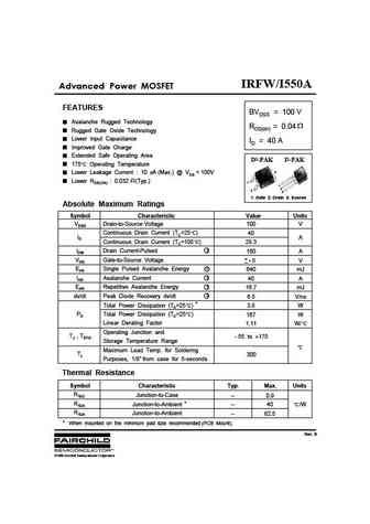
IRFW/I550A Advanced Power MOSFET FEATURES BVDSS = 100 V Avalanche Rugged Technology RDS(on) = 0.04 Rugged Gate Oxide Technology Lower Input Capacitance ID = 40 A Improved Gate Charge Extended Safe Operating Area D2-PAK I2-PAK 175 C Operating Temperature 2 A (Max.) @ VDS = 100V Lower Leakage Current 10 Lower RDS(ON) 0.032 (Typ.) 1 1 2 3 3 1. Gat... See More ⇒
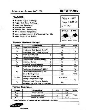
9.5. Size:508K samsung
irfw530a.pdf

Advanced Power MOSFET FEATURES BVDSS = 100 V Avalanche Rugged Technology RDS(on) = 0.11 Rugged Gate Oxide Technology Lower Input Capacitance ID = 14 A Improved Gate Charge Extended Safe Operating Area 175 Operating Temperature 2 Lower Leakage Current 10 A (Max.) @ VDS = 100V Lower RDS(ON) 0.092 (Typ.) 1 1 2 3 3 1. Gate 2. Drain 3. Source Abs... See More ⇒
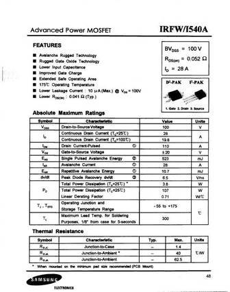
9.6. Size:508K samsung
irfw540a.pdf

Advanced Power MOSFET FEATURES BVDSS = 100 V Avalanche Rugged Technology RDS(on) = 0.052 Rugged Gate Oxide Technology Lower Input Capacitance ID = 28 A Improved Gate Charge Extended Safe Operating Area 175 Operating Temperature 2 Lower Leakage Current 10 A (Max.) @ VDS = 100V Lower RDS(ON) 0.041 (Typ.) 1 1 2 3 3 1. Gate 2. Drain 3. Source Abso... See More ⇒
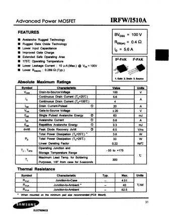
9.7. Size:513K samsung
irfw550a.pdf

Advanced Power MOSFET FEATURES BVDSS = 100 V Avalanche Rugged Technology RDS(on) = 0.04 Rugged Gate Oxide Technology Lower Input Capacitance ID = 40 A Improved Gate Charge Extended Safe Operating Area 175 Operating Temperature 2 Lower Leakage Current 10 A (Max.) @ VDS = 100V Lower RDS(ON) 0.032 (Typ.) 1 1 2 3 3 1. Gate 2. Drain 3. Source Absolute ... See More ⇒
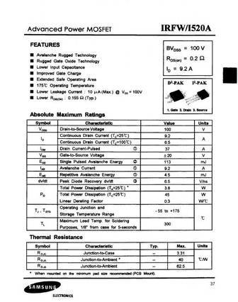
9.8. Size:503K samsung
irfw520a.pdf
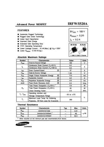
Advanced Power MOSFET FEATURES BVDSS = 100 V Avalanche Rugged Technology RDS(on) = 0.2 Rugged Gate Oxide Technology Lower Input Capacitance ID = 9.2 A Improved Gate Charge Extended Safe Operating Area 175 Operating Temperature 2 Lower Leakage Current 10 A (Max.) @ VDS = 100V Lower RDS(ON) 0.155 (Typ.) 1 1 2 3 3 1. Gate 2. Drain 3. Source Abso... See More ⇒
Detailed specifications: IRFU9210
, IRFU9212
, IRFU9214
, IRFU9220
, IRFU9222
, IRFU9310
, IRFUC20
, IRFW450
, AON6414A
, IRFW520A
, IRFW530A
, IRFW540A
, IRFW550A
, IRFW610A
, IRFW614A
, IRFW620A
, IRFW624A
.
History: RJL6012DPE
Keywords - IRFW510A MOSFET specs
IRFW510A cross reference
IRFW510A equivalent finder
IRFW510A pdf lookup
IRFW510A substitution
IRFW510A replacement
Learn how to find the right MOSFET substitute. A guide to cross-reference, check specs and replace MOSFETs in your circuits.