FQD12N20TM Datasheet. Specs and Replacement
Type Designator: FQD12N20TM 📄📄
Type of Transistor: MOSFET
Type of Control Channel: N-Channel
Absolute Maximum Ratings
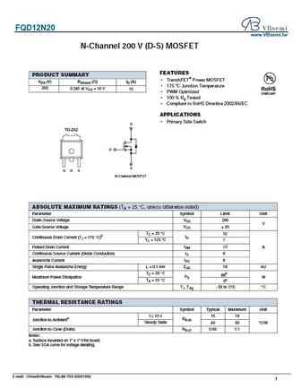
Pd ⓘ - Maximum Power Dissipation: 55 W
|Vds|ⓘ - Maximum Drain-Source Voltage: 200 V
|Vgs|ⓘ - Maximum Gate-Source Voltage: 30 V
|Id| ⓘ - Maximum Drain Current: 9 A
Tj ⓘ - Maximum Junction Temperature: 150 °C
Electrical Characteristics
tr ⓘ - Rise Time: 120 nS
Cossⓘ - Output Capacitance: 125 pF
RDSonⓘ - Maximum Drain-Source On-State Resistance: 0.28 Ohm
Package: D-PAK
📄📄 Copy
FQD12N20TM substitution
- MOSFET ⓘ Cross-Reference Search
FQD12N20TM datasheet
fqd12n20tf fqd12n20tm fqd12n20 fqu12n20 fqu12n20tu.pdf
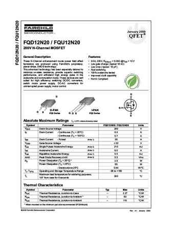
January 2009 QFET FQD12N20 / FQU12N20 200V N-ChanneI MOSFET GeneraI Description Features These N-Channel enhancement mode power field effect 9.0A, 200V, RDS(on) = 0.28 @VGS = 10 V transistors are produced using Fairchild s proprietary, Low gate charge ( typical 18 nC) planar stripe, DMOS technology. Low Crss ( typical 18 pF) This advanced technology has been especia... See More ⇒
fqd12n20ltm f085.pdf
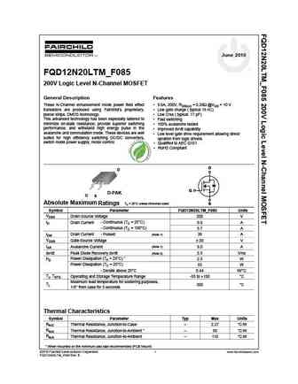
June 2010 FQD12N20LTM_F085 200V Logic Level N-Channel MOSFET General Description Features These N-Channel enhancement mode power field effect 9.0A, 200V, RDS(on) = 0.28 @VGS = 10 V transistors are produced using Fairchild s proprietary, Low gate charge ( typical 16 nC) planar stripe, DMOS technology. Low Crss ( typical 17 pF) This advanced technology has been especiall... See More ⇒
fqd12n20ltf fqd12n20ltm fqd12n20l fqu12n20l.pdf
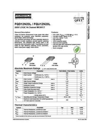
January 2009 QFET FQD12N20L / FQU12N20L 200V LOGIC N-Channel MOSFET General Description Features These N-Channel enhancement mode power field effect 9.0A, 200V, RDS(on) = 0.28 @VGS = 10 V transistors are produced using Fairchild s proprietary, Low gate charge ( typical 16 nC) planar stripe, DMOS technology. Low Crss ( typical 17 pF) This advanced technology has been ... See More ⇒
fqd12n20l.pdf
Is Now Part of To learn more about ON Semiconductor, please visit our website at www.onsemi.com Please note As part of the Fairchild Semiconductor integration, some of the Fairchild orderable part numbers will need to change in order to meet ON Semiconductor s system requirements. Since the ON Semiconductor product management systems do not have the ability to manage part nomenclatur... See More ⇒
Detailed specifications: FQD10N20LTM, FQD10N20TF, FQD10N20TM, FQD11P06TF, FQD11P06TM, FQD12N20LTF, FQD12N20LTM, FQD12N20TF, FTP08N06A, FQD12P10TF, FQD12P10TM, FQD13N06LTF, FQD13N06LTM, FQD13N06TF, FQD13N06TM, FQD13N10TF, FQD13N10TM
Keywords - FQD12N20TM MOSFET specs
FQD12N20TM cross reference
FQD12N20TM equivalent finder
FQD12N20TM pdf lookup
FQD12N20TM substitution
FQD12N20TM replacement
Need a MOSFET replacement? Our guide shows you how to find a perfect substitute by comparing key parameters and specs
MOSFET Parameters. How They Affect Each Other
History: NVD20N03L27 | HM70P03K | AGM12T08A | IXFH70N20Q3 | FDD5N50U | DHS020N04P | AGM13T30A
🌐 : EN ES РУ
LIST
Last Update
MOSFET: CS95118 | CS85105A | CS75N45 | CS72N12 | CS55N50 | CS48N75A | CS40N27 | MSQ60P04D | MSQ40P07D | MSQ30P40D
Popular searches
2sc485 | 2sd287 | 2sd438 | a1492 | hy4008 | ncep039n10m | 20n50 | 2sc869


