SD202DC Datasheet. Specs and Replacement
Type Designator: SD202DC 📄📄
Type of Transistor: MOSFET
Type of Control Channel: N-Channel
Absolute Maximum Ratings
Pd ⓘ - Maximum Power Dissipation: 0.36 W
|Vds|ⓘ - Maximum Drain-Source Voltage: 20 V
|Vgs|ⓘ - Maximum Gate-Source Voltage: 40 V
|Id| ⓘ - Maximum Drain Current: 0.05 A
Tj ⓘ - Maximum Junction Temperature: 125 °C
Electrical Characteristics
Cossⓘ - Output Capacitance: 1 pF
RDSonⓘ - Maximum Drain-Source On-State Resistance: 50 Ohm
Package: TO-52
📄📄 Copy
- MOSFET ⓘ Cross-Reference Search
SD202DC datasheet
..1. Size:26K calogic
sd200dc sd201dc sd202dc sd203dc sstsd201 sstsd203.pdf 
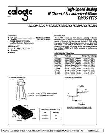
High-Speed Analog N-Channel Enhancement-Mode LLC DMOS FETS SD200 / SD201 / SD202 / SD203 / SSTSD201 / SSTSD203 FEATURES DESCRIPTION High gain . . . . . . . . . . . . . . . . . . . . . 8.0 dB min @ 1 GHz The SD200 series is manufactured utilizing Calogic s Low Noise. . . . . . . . . . . . . . . . . . . . . 5.0 dB max @ 1 GHz proprietary DMOS design and processing techniques... See More ⇒
9.1. Size:91K sanyo
2sd2028.pdf
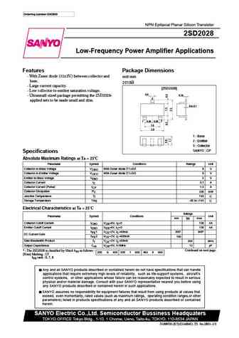
Ordering number EN2803 NPN Epitaxial Planar Silicon Transistor 2SD2028 Low-Frequency Power Amplifier Applications Features Package Dimensions With Zener diode (11 3V) between collector and unit mm base. 2018B Large current capacity. [2SD2028] Low collector-to-emitter saturation voltage. 0.4 Ultrasmall-sized package permitting the 2SD2028- 0.16 3 applied sets to ... See More ⇒
9.2. Size:371K samsung
ssd2021.pdf

I I I I 8 SOIC FEATURES 8 S1 1 D1 G1 2 7 D1 3 6 S2 D2 Lower RDS(ON) 5 G2 4 D2 Improved Inductive Ruggedness Top View Fast Swtching Times D1 D1 Low Input Capacitance Extended Safe Operating Area Improved High Temperature Reliability G1 Product Summary Part Number BVdss Rds(on) ID S1 SSD2021 30V 0.05 5.0A N -Channel MOSFET Absolute Maximum ... See More ⇒
9.3. Size:363K samsung
ssd2025.pdf
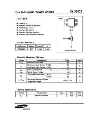
I I I I 8 SOIC FEATURES 8 S1 1 D1 G1 2 7 D1 3 6 S2 D2 Lower RDS(ON) 5 G2 4 D2 Improved Inductive Ruggedness Top View Fast Swtching Times D1 D1 Low Input Capacitance Extended Safe Operating Area Improved High Temperature Reliability G1 Product Summary Part Number BVdss Rds(on) ID S1 SSD2025 60V 0.10 3.3A N -Channel MOSFET Absolute Maximum ... See More ⇒
9.4. Size:54K panasonic
2sd2029.pdf
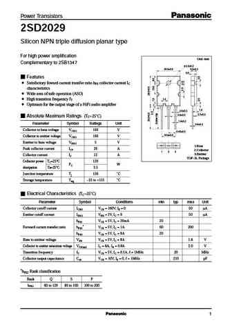
Power Transistors 2SD2029 Silicon NPN triple diffusion planar type For high power amplification Unit mm Complementary to 2SB1347 3.3 0.2 20.0 0.5 5.0 0.3 3.0 Features Satisfactory foward current transfer ratio hFE collector current IC characteristics Wide area of safe operation (ASO) 1.5 High transition frequency fT Optimum for the output stage of a HiFi audio amplifie... See More ⇒
9.5. Size:1107K kexin
2sd2028.pdf
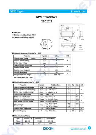
SMD Type Transistors NPN Transistors 2SD2028 SOT-23 Unit mm +0.1 2.9-0.1 +0.1 0.4 -0.1 3 Features Collector Current Capability IC=700mA Collector Emitter Voltage VCEO=8V 1 2 +0.1 +0.05 0.95 -0.1 0.1 -0.01 1.9+0.1 -0.1 1.Base 2.Emitter 3.collector Absolute Maximum Ratings Ta = 25 Parameter Symbol Rating Unit Collector - Base Voltage (Note.1) VCBO 8 ... See More ⇒
9.6. Size:209K inchange semiconductor
2sd2024.pdf
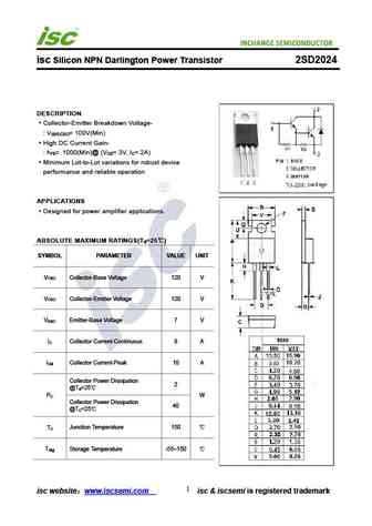
isc Silicon NPN Darlington Power Transistor 2SD2024 DESCRIPTION Collector-Emitter Breakdown Voltage- V = 100V(Min) (BR)CEO High DC Current Gain- h = 1000(Min)@ (V = 3V, I = 2A) FE CE C Minimum Lot-to-Lot variations for robust device performance and reliable operation APPLICATIONS Designed for power amplifier applications. ABSOLUTE MAXIMUM RATINGS(T =25 ) a SYMBOL PAR... See More ⇒
9.7. Size:209K inchange semiconductor
2sd2027.pdf
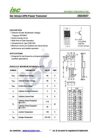
isc Silicon NPN Power Transistor 2SD2027 DESCRIPTION Collector-Emitter Breakdown Voltage- V = 60V(Min) (BR)CEO Good Linearity of h FE Wide Area of Safe Operation Complement to Type 2SB1346 Minimum Lot-to-Lot variations for robust device performance and reliable operation APPLICATIONS Designed for low frequency and general purpose amplifier applications. ABSOLUTE MAXI... See More ⇒
9.8. Size:180K inchange semiconductor
2sd2021.pdf
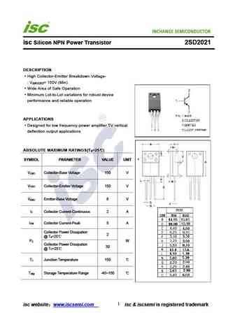
INCHANGE Semiconductor isc Silicon NPN Power Transistor 2SD2021 DESCRIPTION High Collector-Emitter Breakdown Voltage- V = 150V (Min) (BR)CEO Wide Area of Safe Operation Minimum Lot-to-Lot variations for robust device performance and reliable operation APPLICATIONS Designed for low frequency power amplifier TV vertical deflection output applications ABSOLUTE MAXIMUM RATINGS... See More ⇒
9.9. Size:182K inchange semiconductor
2sd2020.pdf
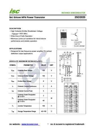
INCHANGE Semiconductor isc Silicon NPN Power Transistor 2SD2020 DESCRIPTION High Collector-Emitter Breakdown Voltage- V = 150V (Min) (BR)CEO Wide Area of Safe Operation Minimum Lot-to-Lot variations for robust device performance and reliable operation APPLICATIONS Designed for low frequency power amplifier TV vertical deflection output applications ABSOLUTE MAXIMUM RATINGS... See More ⇒
9.10. Size:209K inchange semiconductor
2sd2023.pdf
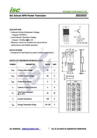
isc Silicon NPN Power Transistor 2SD2023 DESCRIPTION Collector-Emitter Breakdown Voltage- V = 60V(Min.) (BR)CEO Low Collector Saturation Voltage V = 1.5V(Max)@I = 2A CE(sat) C Minimum Lot-to-Lot variations for robust device performance and reliable operation APPLICATIONS Designed for low frequency power amplifier applications. ABSOLUTE MAXIMUM RATINGS(T =25 ) a SYMBO... See More ⇒
9.11. Size:187K inchange semiconductor
2sd2022.pdf
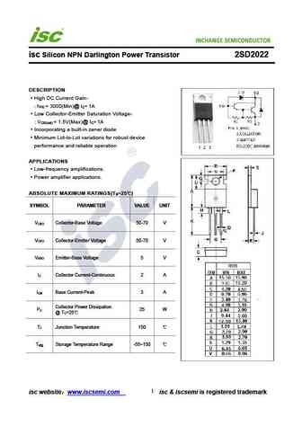
INCHANGE Semiconductor isc Silicon NPN Darlington Power Transistor 2SD2022 DESCRIPTION High DC Current Gain- h = 3000(Min)@ I = 1A FE C Low Collector-Emitter Saturation Voltage- V = 1.5V(Max)@ I = 1A CE(sat) C Incorporating a built-in zener diode Minimum Lot-to-Lot variations for robust device performance and reliable operation APPLICATIONS Low-frequency amplification... See More ⇒
9.12. Size:212K inchange semiconductor
2sd2025.pdf
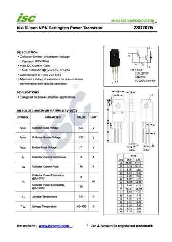
isc Silicon NPN Darlington Power Transistor 2SD2025 DESCRIPTION Collector-Emitter Breakdown Voltage- V = 100V(Min) (BR)CEO High DC Current Gain- h = 1000(Min)@ (V = 3V, I = 2A) FE CE C Complement to Type 2SB1344 Minimum Lot-to-Lot variations for robust device performance and reliable operation APPLICATIONS Designed for power amplifier applications. ABSOLUTE MAXIMUM RA... See More ⇒
9.13. Size:216K inchange semiconductor
2sd2029.pdf
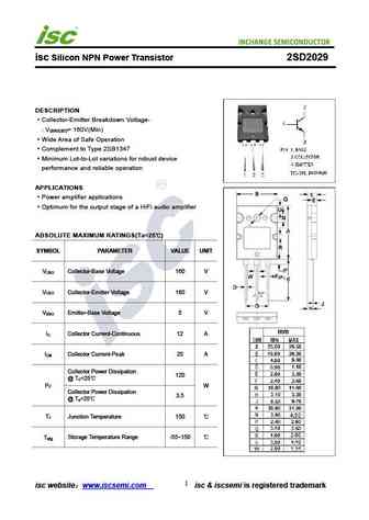
isc Silicon NPN Power Transistor 2SD2029 DESCRIPTION Collector-Emitter Breakdown Voltage- V = 160V(Min) (BR)CEO Wide Area of Safe Operation Complement to Type 2SB1347 Minimum Lot-to-Lot variations for robust device performance and reliable operation APPLICATIONS Power amplifier applications Optimum for the output stage of a HiFi audio amplifier ABSOLUTE MAXIMUM RATINGS... See More ⇒
Detailed specifications: IRF7342QPBF, IRF7343IPBF, IRF7343QPBF, IRF734PBF, IRF7351PBF, SD10425, SD200DC, SD201DC, 2N7000, SD203DC, SD210, SD2100, SD210DE, SD212, SD212DE, SD214, SD214DE
Keywords - SD202DC MOSFET specs
SD202DC cross reference
SD202DC equivalent finder
SD202DC pdf lookup
SD202DC substitution
SD202DC replacement
Need a MOSFET replacement?
Our guide shows you how to find a perfect substitute by comparing key parameters and specs
