IRF9317PBF Datasheet. Specs and Replacement
Type Designator: IRF9317PBF 📄📄
Type of Transistor: MOSFET
Type of Control Channel: P-Channel
Absolute Maximum Ratings
Pd ⓘ - Maximum Power Dissipation: 2.5 W
|Vds|ⓘ - Maximum Drain-Source Voltage: 30 V
|Vgs|ⓘ - Maximum Gate-Source Voltage: 20 V
|Id| ⓘ - Maximum Drain Current: 16 A
Tj ⓘ - Maximum Junction Temperature: 150 °C
Electrical Characteristics
tr ⓘ - Rise Time: 64 nS
Cossⓘ - Output Capacitance: 640 pF
RDSonⓘ - Maximum Drain-Source On-State Resistance: 0.0066 Ohm
Package: SO-8
📄📄 Copy
IRF9317PBF substitution
- MOSFET ⓘ Cross-Reference Search
IRF9317PBF datasheet
irf9317pbf.pdf
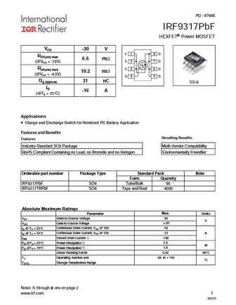
PD - 97465 IRF9317PbF HEXFET Power MOSFET VDS -30 V S 18 D RDS(on) max 6.6 m S 27 D (@VGS = -10V) RDS(on) max S 3 6 D 10.2 m (@VGS = -4.5V) G 4 5 D Qg (typical) 31 nC SO-8 ID -16 A (@TA = 25 C) Applications Charge and Discharge Switch for Notebook PC Battery Application Features and Benefits Resulting Benefits Features Industry-Standard SO8 Package Multi-Vendor... See More ⇒
irf9317tr.pdf
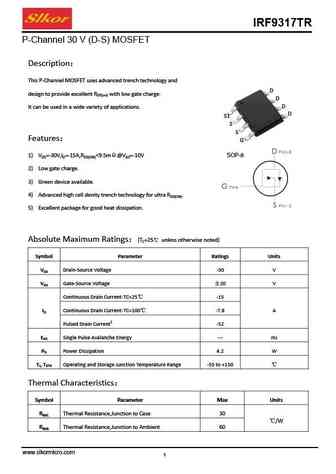
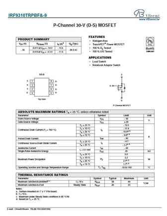
IRF9317TR P-Channel 30 V (D-S) MOSFET Description This P-Channel MOSFET uses advanced trench technology and D design to provide excellent RDS(on) with low gate charge. D D It can be used in a wide variety of applications. D S1 S S Features G 1) VDS=-30V,ID=-15A,RDS(ON)... See More ⇒
irf9310pbf-1.pdf
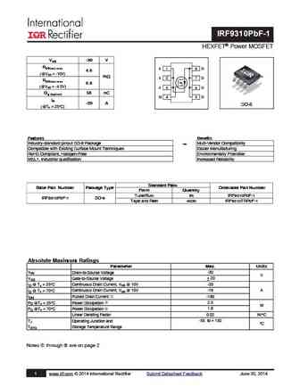
IRF9310PbF-1 HEXFET Power MOSFET VDS -30 V RDS(on) max S 18 D 4.6 (@V = -10V) GS m S 27 D RDS(on) max 6.8 (@V = -4.5V) GS S 3 6 D Qg (typical) 58 nC G 4 5 D ID -20 A SO-8 (@T = 25 C) A Features Benefits Industry-standard pinout SO-8 Package Multi-Vendor Compatibility Compatible with Existing Surface Mount Techniques Easier Manufacturing RoHS Compliant, Halo... See More ⇒
irf9310pbf.pdf
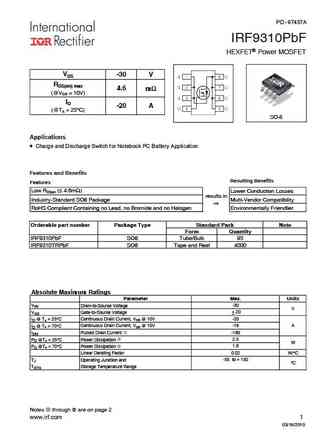
PD - 97437A IRF9310PbF HEXFET Power MOSFET VDS -30 V RDS(on) max 4.6 m (@VGS = 10V) ID -20 A (@TA = 25 C) SO-8 Applications Charge and Discharge Switch for Notebook PC Battery Application Features and Benefits Resulting Benefits Features Low RDSon ( 4.6m ) Lower Conduction Losses results in Industry-Standard SO8 Package Multi-Vendor Compatibility RoHS ... See More ⇒
Detailed specifications: IRF8788PBF-1, IRF8852PBF, IRF8910GPBF, IRF8910PBF-1, IRF9130SMD, IRF9130SMD05, IRF9310PBF, IRF9310PBF-1, IRF540N, IRF9321PBF, IRF9328PBF, IRF9332PBF, IRF9333PBF, IRF9335PBF, IRF9358PBF, IRF9362PBF, IRF9383MPBF
Keywords - IRF9317PBF MOSFET specs
IRF9317PBF cross reference
IRF9317PBF equivalent finder
IRF9317PBF pdf lookup
IRF9317PBF substitution
IRF9317PBF replacement
Step-by-step guide to finding a MOSFET replacement. Cross-reference parts and ensure compatibility for your repair or project.
MOSFET Parameters. How They Affect Each Other
History: IRF9310PBF-1 | IRF9321PBF | CED2303 | IRFZ34PBF
🌐 : EN ES РУ
LIST
Last Update
MOSFET: CEM3139 | CEM3133 | CEM3115 | CED3133 | CEC3257 | CEC2533 | CEB100N10L | BC3134KT | BC3134K | BC2302W
Popular searches
30g124 | 75339p mosfet | a968 transistor | f1010e mosfet | 2sc3883 | c3306 datasheet | hy3810 | c711 transistor
