STN4102 Specs and Replacement
Type Designator: STN4102
Type of Transistor: MOSFET
Type of Control Channel: N -Channel
Absolute Maximum Ratings
Pd ⓘ - Maximum Power Dissipation: 25 W
|Vds|ⓘ - Maximum Drain-Source Voltage: 30 V
|Vgs|ⓘ - Maximum Gate-Source Voltage: 20 V
|Id| ⓘ - Maximum Drain Current: 15 A
Tj ⓘ - Maximum Junction Temperature: 150 °C
Electrical Characteristics
tr ⓘ - Rise Time: 3.7 nS
Cossⓘ - Output Capacitance: 60 pF
Rds ⓘ - Maximum Drain-Source On-State Resistance: 0.032 Ohm
Package: TO-251 TO-252
STN4102 substitution
STN4102 datasheet
stn4102.pdf
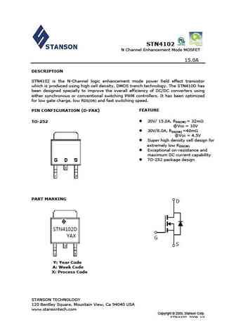
STN4102 N Channel Enhancement Mode MOSFET 15.0A DESCRIPTION STN4102 is the N-Channel logic enhancement mode power field effect transistor which is produced using high cell density, DMOS trench technology. The STN410D has been designed specially to improve the overall efficiency of DC/DC converters using either synchronous or conventional switching PWM controllers. It has been op... See More ⇒
stn410d.pdf
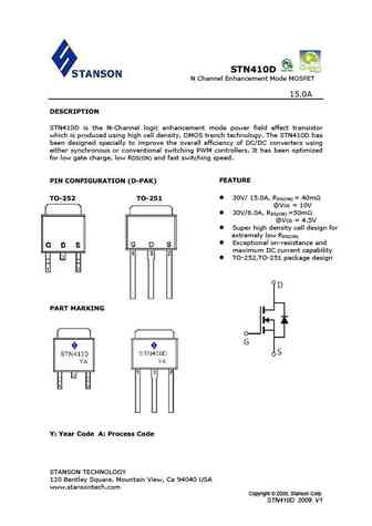
STN410D N Channel Enhancement Mode MOSFET 15.0A DESCRIPTION STN410D is the N-Channel logic enhancement mode power field effect transistor which is produced using high cell density, DMOS trench technology. The STN410D has been designed specially to improve the overall efficiency of DC/DC converters using either synchronous or conventional switching PWM controllers. It has been o... See More ⇒
stn4110.pdf
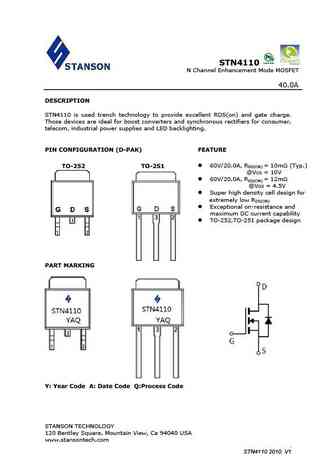
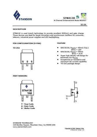
STN4110 N Channel Enhancement Mode MOSFET 40.0A DESCRIPTION STN4110 is used trench technology to provide excellent RDS(on) and gate charge. Those devices are ideal for boost converters and synchronous rectifiers for consumer, telecom, industrial power supplies and LED backlighting. PIN CONFIGURATION (D-PAK) FEATURE 60V/20.0A, RDS(ON) = 10m (Typ.) TO-252 TO-251 @VGS = ... See More ⇒
stn4186d.pdf
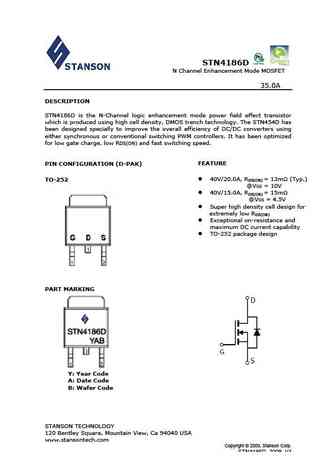
STN4186D N Channel Enhancement Mode MOSFET 35.0A DESCRIPTION STN4186D is the N-Channel logic enhancement mode power field effect transistor which is produced using high cell density, DMOS trench technology. The STN454D has been designed specially to improve the overall efficiency of DC/DC converters using either synchronous or conventional switching PWM controllers. It has been o... See More ⇒
Detailed specifications: STN3400 , STN3400A , STN3404 , STN3406 , STN3414 , STN3446 , STN3456 , STN3P6F6 , IRF730 , STN410D , STN4110 , STN4130 , STN4186D , STN4189D , STN4346 , STN4392 , STN4402 .
History: BUK9675-55A | HM3205B
Keywords - STN4102 MOSFET specs
STN4102 cross reference
STN4102 equivalent finder
STN4102 pdf lookup
STN4102 substitution
STN4102 replacement
Step-by-step guide to finding a MOSFET replacement. Cross-reference parts and ensure compatibility for your repair or project.

History: BUK9675-55A | HM3205B


LIST
Last Update
MOSFET: AOK065V65X2 | AOK065V120X2 | AOK033V120X2Q | AOK033V120X2 | AOB380A60L | AOB29S50L | AO3481C | AO3480 | APG068N04Q | APG068N04G
Popular searches
tip117 | 2n3643 | 2sc2078 transistor equivalent | 2sc2073 | a608 transistor | c536 transistor | 2n706 | 2n388