ST2341S23RG Specs and Replacement
Type Designator: ST2341S23RG
Type of Transistor: MOSFET
Type of Control Channel: P-Channel
Absolute Maximum Ratings
Pd ⓘ - Maximum Power Dissipation: 1.25 W
|Vds|ⓘ - Maximum Drain-Source Voltage: 20 V
|Vgs|ⓘ - Maximum Gate-Source Voltage: 12 V
|Id| ⓘ - Maximum Drain Current: 5.3 A
Tj ⓘ - Maximum Junction Temperature: 150 °C
Electrical Characteristics
tr ⓘ - Rise Time: 35 nS
Cossⓘ - Output Capacitance: 160 pF
RDSonⓘ - Maximum Drain-Source On-State Resistance: 0.04 Ohm
Package: SOT-23
ST2341S23RG substitution
- MOSFET ⓘ Cross-Reference Search
ST2341S23RG datasheet
st2341s23rg.pdf
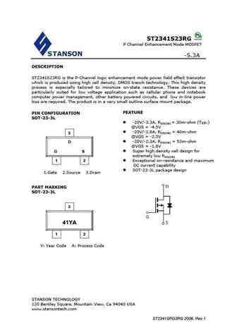
ST2341S23RG P Channel Enhancement Mode MOSFET -5.3A DESCRIPTION ST2341S23RG is the P-Channel logic enhancement mode power field effect transistor which is produced using high cell density, DMOS trench technology. This high density process is especially tailored to minimize on-state resistance. These devices are particularly suited for low voltage application such as cellular pho... See More ⇒
st2341s23r.pdf
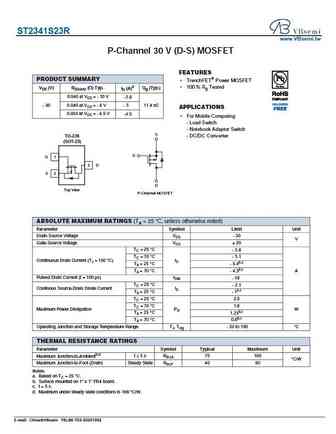
ST2341S23R www.VBsemi.tw P-Channel 30 V (D-S) MOSFET FEATURES PRODUCT SUMMARY TrenchFET Power MOSFET 100 % Rg Tested VDS (V) RDS(on) ( ) Typ. ID (A)a Qg (Typ.) 0.046 at VGS = - 10 V - 5.6 0.049 at VGS = - 6 V - 5 11.4 nC - 30 APPLICATIONS 0.054 at VGS = - 4.5 V -4.5 For Mobile Computing - Load Switch - Notebook Adaptor Switch S TO-236 - DC/DC Converter (SOT-... See More ⇒
st2341srg.pdf
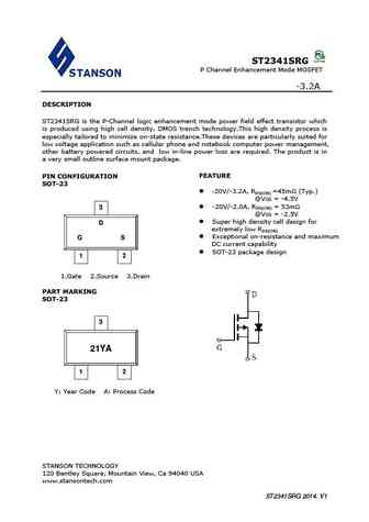
ST2341SRG P Channel Enhancement Mode MOSFET -3.2A DESCRIPTION ST2341SRG is the P-Channel logic enhancement mode power field effect transistor which is produced using high cell density, DMOS trench technology.This high density process is especially tailored to minimize on-state resistance.These devices are particularly suited for low voltage application such as cellular phone and... See More ⇒
st2341a.pdf
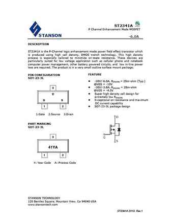
ST2341A P Channel Enhancement Mode MOSFET -6.0A DESCRIPTION ST2341A is the P-Channel logic enhancement mode power field effect transistor which is produced using high cell density, DMOS trench technology. This high density process is especially tailored to minimize on-state resistance. These devices are particularly suited for low voltage application such as cellular phone and n... See More ⇒
Detailed specifications: ST2303SRG, ST2304, ST2304SRG, ST2305, ST2305A, ST2318SRG, ST2319SRG, ST2341A, IRF630, ST2342, ST25N10, ST3400S23RG, ST3400SRG, ST3401M23RG, ST3401SRG, ST3406, ST3406SRG
Keywords - ST2341S23RG MOSFET specs
ST2341S23RG cross reference
ST2341S23RG equivalent finder
ST2341S23RG pdf lookup
ST2341S23RG substitution
ST2341S23RG replacement
Step-by-step guide to finding a MOSFET replacement. Cross-reference parts and ensure compatibility for your repair or project.


