HFB1N60S Specs and Replacement
Type Designator: HFB1N60S
Type of Transistor: MOSFET
Type of Control Channel: N-Channel
Absolute Maximum Ratings
Pd ⓘ - Maximum Power Dissipation: 0.9 W
|Vds|ⓘ - Maximum Drain-Source Voltage: 600 V
|Vgs|ⓘ - Maximum Gate-Source Voltage: 30 V
|Id| ⓘ - Maximum Drain Current: 0.3 A
Tj ⓘ - Maximum Junction Temperature: 150 °C
Electrical Characteristics
tr ⓘ - Rise Time: 21 nS
Cossⓘ - Output Capacitance: 22 pF
RDSonⓘ - Maximum Drain-Source On-State Resistance: 12 Ohm
Package: TO-92
HFB1N60S substitution
- MOSFET ⓘ Cross-Reference Search
HFB1N60S datasheet
hfb1n60s.pdf

Sep 2009 BVDSS = 600 V RDS(on) typ HFB1N60S ID = 0.3 A 600V N-Channel MOSFET TO-92 FEATURES 1 Originative New Design 2 3 Superior Avalanche Rugged Technology 1.Gate 2. Drain 3. Source Robust Gate Oxide Technology D Very Low Intrinsic Capacitances Excellent Switching Characteristics G Unrivalled Gate Charge 3.0 nC (Typ.) Extended Safe Operating Area ... See More ⇒
hfb1n60f.pdf
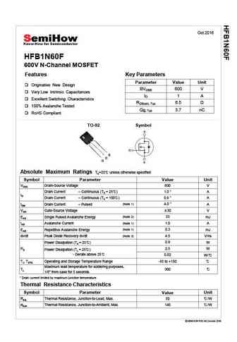
Oct 2016 HFB1N60F 600V N-Channel MOSFET Features Key Parameters Parameter Value Unit Originative New Design BVDSS 600 V Very Low Intrinsic Capacitances ID 1A Excellent Switching Characteristics RDS(on), Typ 6.5 100% Avalanche Tested Qg, Typ 3.7 nC RoHS Compliant TO-92 Symbol S D G Absolute Maximum Ratings TC=25 unless otherwise specified Symbol Parameter Value Uni... See More ⇒
hfb1n65s.pdf
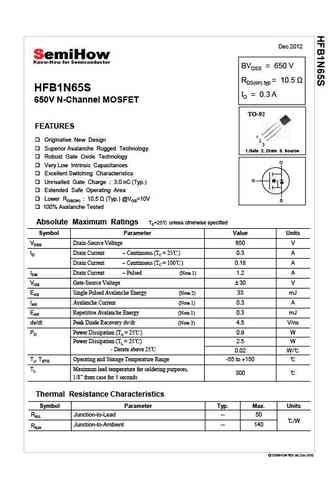
Dec 2012 BVDSS = 650 V RDS(on) typ HFB1N65S ID = 0.3 A 650V N-Channel MOSFET TO-92 FEATURES 1 Originative New Design 2 3 Superior Avalanche Rugged Technology 1.Gate 2. Drain 3. Source Robust Gate Oxide Technology D Very Low Intrinsic Capacitances Excellent Switching Characteristics G Unrivalled Gate Charge 3.0 nC (Typ.) Extended Safe Operating Area... See More ⇒
hfb1n70s.pdf
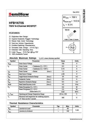
Dec 2012 BVDSS = 700 V RDS(on) typ HFB1N70S ID = 0.3 A 700V N-Channel MOSFET TO-92 FEATURES 1 Originative New Design 2 3 Superior Avalanche Rugged Technology 1.Gate 2. Drain 3. Source Robust Gate Oxide Technology D Very Low Intrinsic Capacitances Excellent Switching Characteristics G Unrivalled Gate Charge 3.5 nC (Typ.) Extended Safe Operating Area... See More ⇒
Detailed specifications: HCP20NT60V, HCS12NK65V, HCS20NT60V, HCT7000M, HCT7000MTXV, HCU6N70S, HCU7NE70S, HFA9N90, IRFP250, HFB1N65S, HFB1N70S, HFD1N60S, HFD1N65S, HFD2N60, HFD2N60S, HFD2N60U, HFD2N65S
Keywords - HFB1N60S MOSFET specs
HFB1N60S cross reference
HFB1N60S equivalent finder
HFB1N60S pdf lookup
HFB1N60S substitution
HFB1N60S replacement
Learn how to find the right MOSFET substitute. A guide to cross-reference, check specs and replace MOSFETs in your circuits.
🌐 : EN ES РУ

LIST
Last Update
MOSFET: CM4407 | CM3407 | CM3400 | SVF11N65F | SVF11N65T | FKBB3105 | EHBA036R1 | CRTT067N10N | AP6NA3R2MT | AP65SA145DDT8
Popular searches
mp38a | bc546 transistor | bd243 | 2sk170 datasheet | 2n7000 equivalent | tip31 | tip122 transistor | 2sc1079