CS13N50FA9H Datasheet. Specs and Replacement
Type Designator: CS13N50FA9H 📄📄
Type of Transistor: MOSFET
Type of Control Channel: N-Channel
Absolute Maximum Ratings
Pd ⓘ - Maximum Power Dissipation: 60 W
|Vds|ⓘ - Maximum Drain-Source Voltage: 500 V
|Vgs|ⓘ - Maximum Gate-Source Voltage: 30 V
|Id| ⓘ - Maximum Drain Current: 13 A
Tj ⓘ - Maximum Junction Temperature: 150 °C
Electrical Characteristics
tr ⓘ - Rise Time: 27 nS
Cossⓘ - Output Capacitance: 210 pF
RDSonⓘ - Maximum Drain-Source On-State Resistance: 0.45 Ohm
Package: TO-220F
📄📄 Copy
CS13N50FA9H substitution
- MOSFET ⓘ Cross-Reference Search
CS13N50FA9H datasheet
cs13n50fa9h.pdf
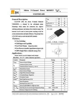
Silicon N-Channel Power MOSFET R CS13N50F A9H VDSS 500 V General Description ID 13 A CS13N50F A9H, the silicon N-channel Enhanced PD (TC=25 ) 60 W VDMOSFETs, is obtained by the self-aligned planar RDS(ON)Typ 0.34 Technology which reduce the conduction loss, improve switching performance and enhance the avalanche energy. The transistor can be used in variou... See More ⇒
cs13n50fa9r.pdf
Silicon N-Channel Power MOSFET R CS13N50F A9R General Description VDSS 500 V CS13N50F A9R, the silicon N-channel Enhanced ID 13 A PD(TC=25 ) 42 W VDMOSFETs, is obtained by the self-aligned planar Technology RDS(ON)Typ 0.4 which reduce the conduction loss, improve switching performance and enhance the avalanche energy. The transistor can be used in various po... See More ⇒
jcs13n50ft.pdf
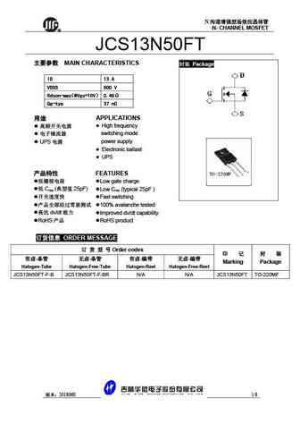
N N- CHANNEL MOSFET R JCS13N50FT MAIN CHARACTERISTICS Package ID 13 A VDSS 500 V Rdson-max @Vgs=10V 0.46 Qg-typ 37 nC APPLICATIONS High frequency switching mode power supply UPS Electronic ballast UPS FEATUR... See More ⇒


Detailed specifications: CS12N60F, CS12N60FA9H, CS12N60FA9HD, CS12N65A8H, CS12N65FA9H, CS138, CS13N15D, CS13N50A8H, AO3407, CS1405, CS140N10A, CS150, CS150N03A8, CS150N04A8, CS15N60, CS16N60A8H, CS19N40A8H
Keywords - CS13N50FA9H MOSFET specs
CS13N50FA9H cross reference
CS13N50FA9H equivalent finder
CS13N50FA9H pdf lookup
CS13N50FA9H substitution
CS13N50FA9H replacement
Can't find your MOSFET? Learn how to find a substitute transistor by analyzing voltage, current and package compatibility
MOSFET Parameters. How They Affect Each Other
History: SHD280502
🌐 : EN ES РУ

LIST
Last Update
MOSFET: BC3134KT | BC3134K | BC2302W | BC2302T-2.8A | BC2302-2.8A | BC2301W | BC2301T-2.8A | CB3139KTB | CB2301DW | BC8205
Popular searches
2sd313 replacement | 2n4249 | a1013 transistor | 2sc2705 | bc239 | 2sc3264 | mp38a | bc546 transistor