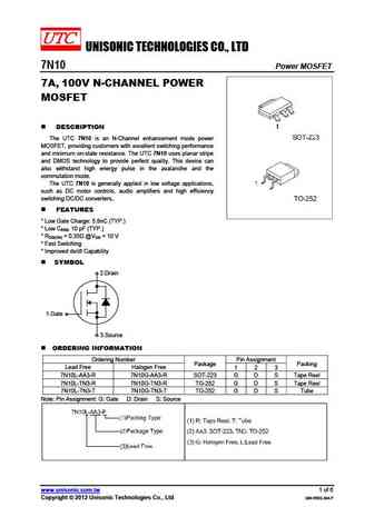
7N10L-AA3 Specs and Replacement
Type Designator: 7N10L-AA3
Type of Transistor: MOSFET
Type of Control Channel: N-Channel
Absolute Maximum Ratings
Pd ⓘ - Maximum Power Dissipation: 2 W
|Vds|ⓘ - Maximum Drain-Source Voltage: 100 V
|Vgs|ⓘ - Maximum Gate-Source Voltage: 25 V
|Id| ⓘ - Maximum Drain Current: 5 A
Tj ⓘ - Maximum Junction Temperature: 150 °C
Electrical Characteristics
tr ⓘ - Rise Time: 24 nS
Cossⓘ - Output Capacitance: 60 pF
Rds ⓘ - Maximum Drain-Source On-State Resistance: 0.35 Ohm
Package: SOT223
7N10L-AA3 substitution
- MOSFET ⓘ Cross-Reference Search
7N10L-AA3 datasheet
fqd7n10ltf fqd7n10ltm fqd7n10l fqu7n10l fqu7n10ltu.pdf
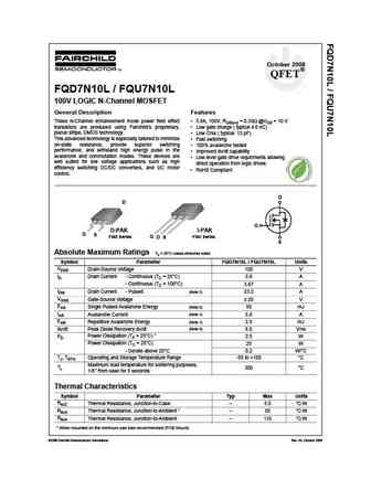
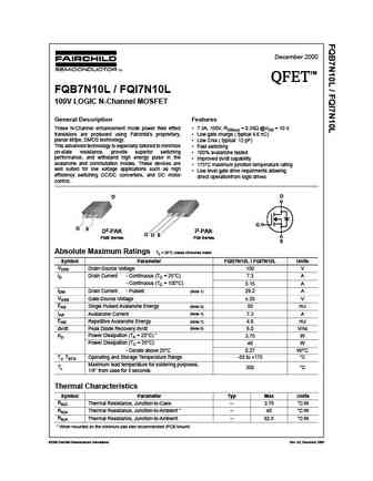
October 2008 QFET FQD7N10L / FQU7N10L 100V LOGIC N-Channel MOSFET General Description Features These N-Channel enhancement mode power field effect 5.8A, 100V, RDS(on) = 0.35 @VGS = 10 V transistors are produced using Fairchild s proprietary, Low gate charge ( typical 4.6 nC) planar stripe, DMOS technology. Low Crss ( typical 12 pF) This advanced technology is especia... See More ⇒
fqp7n10l.pdf
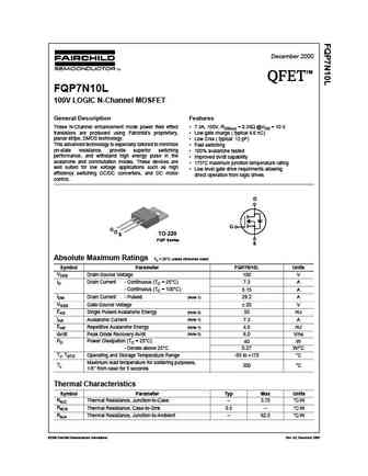
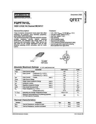
December 2000 TM QFET QFET QFET QFET FQP7N10L 100V LOGIC N-Channel MOSFET General Description Features These N-Channel enhancement mode power field effect 7.3A, 100V, RDS(on) = 0.35 @VGS = 10 V transistors are produced using Fairchild s proprietary, Low gate charge ( typical 4.6 nC) planar stripe, DMOS technology. Low Crss ( typical 12 pF) This advanced technology ... See More ⇒
fqt7n10ltf.pdf
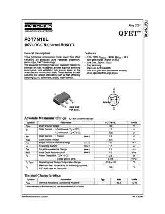
May 2001 TM QFET FQT7N10L 100V LOGIC N-Channel MOSFET General Description Features These N-Channel enhancement mode power field effect 1.7A, 100V, RDS(on) = 0.35 @VGS = 10 V transistors are produced using Fairchild s proprietary, Low gate charge ( typical 4.6 nC) planar stripe, DMOS technology. Low Crss ( typical 12 pF) This advanced technology has been especially tai... See More ⇒
fqt7n10l.pdf

May 2001 TM QFET FQT7N10L 100V LOGIC N-Channel MOSFET General Description Features These N-Channel enhancement mode power field effect 1.7A, 100V, RDS(on) = 0.35 @VGS = 10 V transistors are produced using Fairchild s proprietary, Low gate charge ( typical 4.6 nC) planar stripe, DMOS technology. Low Crss ( typical 12 pF) This advanced technology has been especially tai... See More ⇒

Detailed specifications: APTM50AM24SCG , APTM50AM38SCTG , APTM50DAM38CTG , APTM50HM75SCTG , ATP304 , ATP401 , 2N5670 , 2SK2255-01MR , IRF3205 , 7N10G-AA3 , 7N10L-TN3 , 7N10G-TN3 , AO4466L , AOD4144 , CS60N06C4 , EMB20P03V , FTW20N50A .
Keywords - 7N10L-AA3 MOSFET specs
7N10L-AA3 cross reference
7N10L-AA3 equivalent finder
7N10L-AA3 pdf lookup
7N10L-AA3 substitution
7N10L-AA3 replacement
Need a MOSFET replacement? Our guide shows you how to find a perfect substitute by comparing key parameters and specs
🌐 : EN ES РУ

LIST
Last Update
MOSFET: HAF1008S | HAF1008L | EMZB08P03H | CS30N20FA9R | AOT66613L | AOSP21313C | AOSP21311C | AOB66918L | AO3415C | AOTF20N40L
Popular searches
2sb681 | bc639 equivalent | bd138 transistor equivalent | c1096 transistor | c1345 transistor | jcs640c | kn2907a | ncep028n85 datasheet