NTLJS3180PZTBG Datasheet. Specs and Replacement
Type Designator: NTLJS3180PZTBG 📄📄
Type of Transistor: MOSFET
Type of Control Channel: P-Channel
Absolute Maximum Ratings
Pd ⓘ - Maximum Power Dissipation: 0.7 W
|Vds|ⓘ - Maximum Drain-Source Voltage: 20 V
|Vgs|ⓘ - Maximum Gate-Source Voltage: 8 V
|Id| ⓘ - Maximum Drain Current: 3.5 A
Tj ⓘ - Maximum Junction Temperature: 150 °C
Electrical Characteristics
tr ⓘ - Rise Time: 15 nS
Cossⓘ - Output Capacitance: 180 pF
RDSonⓘ - Maximum Drain-Source On-State Resistance: 0.038 Ohm
Package: WDFN6
NTLJS3180PZTBG substitution
- MOSFET ⓘ Cross-Reference Search
NTLJS3180PZTBG datasheet
ntljs3180pz ntljs3180pztbg.pdf
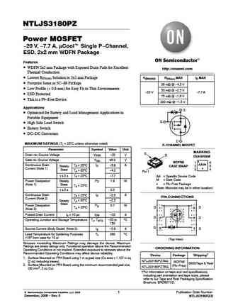
NTLJS3180PZ Power MOSFET -20 V, -7.7 A, mCoolt Single P-Channel, ESD, 2x2 mm WDFN Package Features WDFN 2x2 mm Package with Exposed Drain Pads for Excellent http //onsemi.com Thermal Conduction Lowest RDS(on) Solution in 2x2 mm Package V(BR)DSS RDS(on) MAX ID MAX Footprint Same as SC-88 Package 38 mW @ -4.5 V Low Profile (... See More ⇒
ntljs3113pt1g ntljs3113ptag.pdf
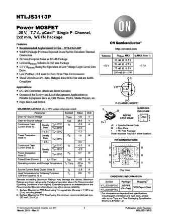
NTLJS3113P Power MOSFET -20 V, -7.7 A, mCoolt Single P-Channel, 2x2 mm, WDFN Package Features Recommended Replacement Device - NTLUS3A40P http //onsemi.com WDFN Package Provides Exposed Drain Pad for Excellent Thermal Conduction V(BR)DSS RDS(on) MAX ID MAX (Note 1) 2x2 mm Footprint Same as SC-88 Package 40 mW @ -4.5 V Lowest RDS(on) Solution in 2x2 mm Package 50 mW @... See More ⇒
ntljs3113p.pdf

NTLJS3113P Power MOSFET -20 V, -7.7 A, mCoolt Single P-Channel, 2x2 mm, WDFN Package Features Recommended Replacement Device - NTLUS3A40P http //onsemi.com WDFN Package Provides Exposed Drain Pad for Excellent Thermal Conduction V(BR)DSS RDS(on) MAX ID MAX (Note 1) 2x2 mm Footprint Same as SC-88 Package 40 mW @ -4.5 V Lowest RDS(on) Solution in 2x2 mm Package 50 mW @... See More ⇒
ntljs3a18pz.pdf
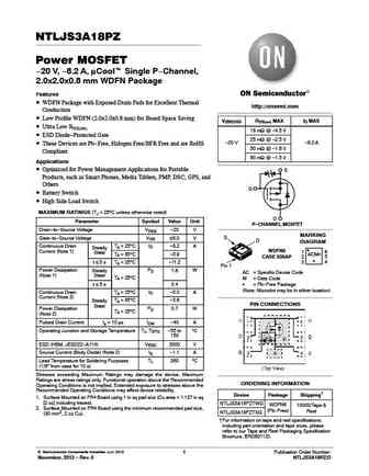
NTLJS3A18PZ Power MOSFET -20 V, -8.2 A, mCoolt Single P-Channel, 2.0x2.0x0.8 mm WDFN Package Features WDFN Package with Exposed Drain Pads for Excellent Thermal http //onsemi.com Conduction Low Profile WDFN (2.0x2.0x0.8 mm) for Board Space Saving V(BR)DSS RDS(on) MAX ID MAX Ultra Low RDS(on) 18 mW @ -4.5 V ESD Diode-Protected Gate 25 mW @ -2.5 V -20 V -8.2 A T... See More ⇒
Detailed specifications: NTLJF4156NT1G, NTLJF4156NTAG, NTLJS1102PTAG, NTLJS1102PTBG, NTLJS2103PTAG, NTLJS2103PTBG, NTLJS3113PT1G, NTLJS3113PTAG, 10N60, NTLJS3A18PZ, NTLJS4114NT1G, NTLJS4149PTAG, NTLJS4159NT1G, NTLLD4901NF, NTLUD3A260PZTAG, NTLUD3A260PZTBG, NTLUD3A50PZ
Keywords - NTLJS3180PZTBG MOSFET specs
NTLJS3180PZTBG cross reference
NTLJS3180PZTBG equivalent finder
NTLJS3180PZTBG pdf lookup
NTLJS3180PZTBG substitution
NTLJS3180PZTBG replacement
Step-by-step guide to finding a MOSFET replacement. Cross-reference parts and ensure compatibility for your repair or project.
