IPB083N15N5LF Specs and Replacement
Type Designator: IPB083N15N5LF
Type of Transistor: MOSFET
Type of Control Channel: N-Channel
Absolute Maximum Ratings
Pd ⓘ - Maximum Power Dissipation: 179 W
|Vds|ⓘ - Maximum Drain-Source Voltage: 150 V
|Vgs|ⓘ - Maximum Gate-Source Voltage: 20 V
|Id| ⓘ - Maximum Drain Current: 105 A
Tj ⓘ - Maximum Junction Temperature: 150 °C
Electrical Characteristics
tr ⓘ - Rise Time: 46 nS
Cossⓘ - Output Capacitance: 740 pF
Rds ⓘ - Maximum Drain-Source On-State Resistance: 0.0083 Ohm
IPB083N15N5LF substitution
- MOSFET ⓘ Cross-Reference Search
IPB083N15N5LF datasheet
ipb083n15n5lf.pdf
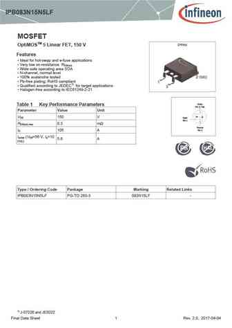
IPB083N15N5LF MOSFET D PAK OptiMOSTM 5 Linear FET, 150 V Features Ideal for hot-swap and e-fuse applications Very low on-resistance R DS(on) Wide safe operating area SOA N-channel, normal level 100% avalanche tested Pb-free plating; RoHS compliant Qualified according to JEDEC1) for target applications Halogen-free according to IEC61249-2-21 Drain ... See More ⇒
ipb083n15n5lf.pdf
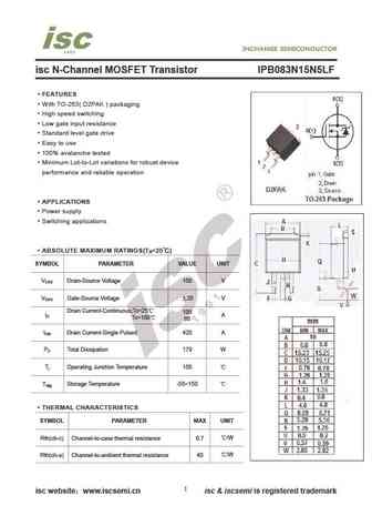
isc N-Channel MOSFET Transistor IPB083N15N5LF FEATURES With TO-263( D2PAK ) packaging High speed switching Low gate input resistance Standard level gate drive Easy to use 100% avalanche tested Minimum Lot-to-Lot variations for robust device performance and reliable operation APPLICATIONS Power supply Switching applications ABSOLUTE MAXIMUM RATINGS(T =25 ) ... See More ⇒
ipp086n10n3g ipi086n10n3g ipb083n10n3g ipd082n10n3g.pdf

IPP086N10N3 G IPI086N10N3 G IPB083N10N3 G IPD082N10N3 G OptiMOS 3 Power-Transistor Product Summary Features VDS 100 V N-channel, normal level RDS(on),max (TO 252) 8.2 mW Excellent gate charge x R product (FOM) DS(on) ID 80 A Very low on-resistance R DS(on) 175 C operating temperature Pb-free lead plating; RoHS compliant Qualified according to JED... See More ⇒
ipp086n10n3-g ipi086n10n3-g ipb083n10n3-g ipd082n10n3-g.pdf
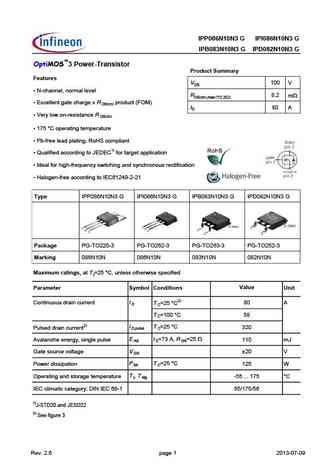
IPP086N10N3 G IPI086N10N3 G IPB083N10N3 G IPD082N10N3 G OptiMOS 3 Power-Transistor Product Summary Features VDS 100 V N-channel, normal level RDS(on),max (TO 252) 8.2 mW Excellent gate charge x R product (FOM) DS(on) ID 80 A Very low on-resistance R DS(on) 175 C operating temperature Pb-free lead plating; RoHS compliant Qualified according to JED... See More ⇒
Detailed specifications: IPB049N06L3 , IPB049NE7N3 , IPB054N06N3 , IPB05CN10N , IPB065N10N3 , IPB067N08N3 , IPB081N06L3 , IPB083N10N3 , IRF840 , IPB097N08N3 , IPB107N20N3 , IPB110N20N3LF , IPB26CN10N , IPB34CN10N , IPB530N15N3 , IPB60R040C7 , IPB60R060C7 .
History: IRF540ZSPBF | WFP840
Keywords - IPB083N15N5LF MOSFET specs
IPB083N15N5LF cross reference
IPB083N15N5LF equivalent finder
IPB083N15N5LF pdf lookup
IPB083N15N5LF substitution
IPB083N15N5LF replacement
Step-by-step guide to finding a MOSFET replacement. Cross-reference parts and ensure compatibility for your repair or project.
History: IRF540ZSPBF | WFP840


LIST
Last Update
MOSFET: AOTF20N40L | AOTF11N60L | AOT11N60L | AONS21303C | AOI280A60 | AOB66914L | AO3485C | AOI780A70 | AOB42S60L | AOTF950A70L
Popular searches
ksc1845 | c1815 transistor | 2sc1815 | irfz44 | 2n5551 | irf540n | irf3205 mosfet | 2n3055