MTD300N20J3 Datasheet. Specs and Replacement
Type Designator: MTD300N20J3 📄📄
Type of Transistor: MOSFET
Type of Control Channel: N-Channel
Absolute Maximum Ratings
Pd ⓘ - Maximum Power Dissipation: 50 W
|Vds|ⓘ - Maximum Drain-Source Voltage: 200 V
|Vgs|ⓘ - Maximum Gate-Source Voltage: 20 V
|Id| ⓘ - Maximum Drain Current: 8.3 A
Tj ⓘ - Maximum Junction Temperature: 150 °C
Electrical Characteristics
tr ⓘ - Rise Time: 7.8 nS
Cossⓘ - Output Capacitance: 46 pF
RDSonⓘ - Maximum Drain-Source On-State Resistance: 0.38 Ohm
Package: TO-252
📄📄 Copy
MTD300N20J3 substitution
- MOSFET ⓘ Cross-Reference Search
MTD300N20J3 datasheet
mtd300n20j3.pdf
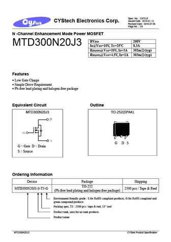
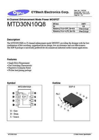
Spec. No. C875J3 Issued Date 2016.01.13 CYStech Electronics Corp. Revised Date 2016.07.06 Page No. 1/9 N -Channel Enhancement Mode Power MOSFET BVDSS 200V MTD300N20J3 ID@VGS=10V, TC=25 C 8.3A RDS(ON)@VGS=10V, ID=3A 302m (typ) RDS(ON)@VGS=4.5V, ID=2A 303m (typ) Features Low Gate Charge Simple Drive Requirement Pb-free lead plating and halogen-... See More ⇒
mtd300n20j3.pdf
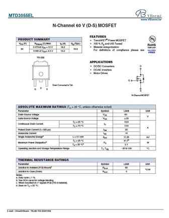
Isc N-Channel MOSFET Transistor MTD300N20J3 FEATURES With To-252(DPAK) package Low input capacitance and gate charge Low gate input resistance 100% avalanche tested Minimum Lot-to-Lot variations for robust device performance and reliable operation APPLICATIONS Switching applications ABSOLUTE MAXIMUM RATINGS(T =25 ) a SYMBOL PARAMETER VALUE UNIT V Drain-Source Vo... See More ⇒
mtd3055vl.pdf
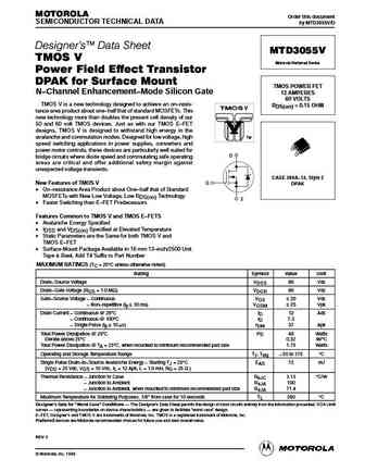
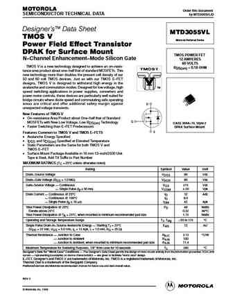
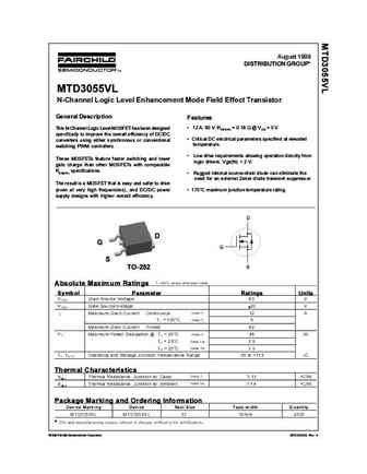
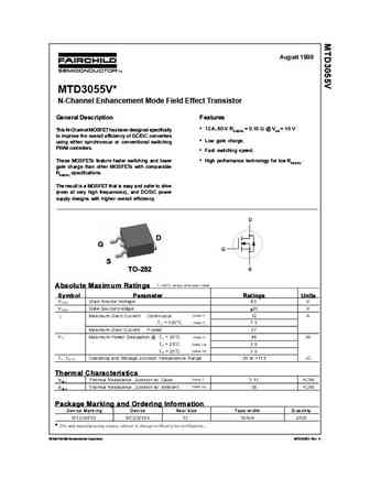
MOTOROLA Order this document SEMICONDUCTOR TECHNICAL DATA by MTD3055VL/D Designer's Data Sheet MTD3055VL TMOS V Motorola Preferred Device Power Field Effect Transistor DPAK for Surface Mount TMOS POWER FET N Channel Enhancement Mode Silicon Gate 12 AMPERES 60 VOLTS TMOS V is a new technology designed to achieve an on resis- RDS(on) = 0.18 OHM tance area product about o... See More ⇒
Detailed specifications: IXFP36N20X3M, IXFP72N20X3M, IXFQ8N85X, IXFY36N20X3, IXTA12N70X2, IXTP230N04T4M, MFT60N12T22FS, MMD60R580QRH, K3569, NTHL040N65S3F, NVD4C05NT4G, IXTH12N70X2, PSMN3R7-100BSE, R6018JNX, SIHG47N60AEF, STD140N6F7, STH140N6F7
Keywords - MTD300N20J3 MOSFET specs
MTD300N20J3 cross reference
MTD300N20J3 equivalent finder
MTD300N20J3 pdf lookup
MTD300N20J3 substitution
MTD300N20J3 replacement
Can't find your MOSFET? Learn how to find a substitute transistor by analyzing voltage, current and package compatibility
MOSFET Parameters. How They Affect Each Other
History: CJAC0410 | 2SJ477-01MR | APQ11BSN40A | APT8090AN | VBE1303 | IXFH22N60P3 | KNB2404A
🌐 : EN ES РУ
LIST
Last Update
MOSFET: CS95118 | CS85105A | CS75N45 | CS72N12 | CS55N50 | CS48N75A | CS40N27 | MSQ60P04D | MSQ40P07D | MSQ30P40D
Popular searches
irf840 datasheet | ge10001 | irf830 | irfp450 | mj21193 | s9014 transistor | bc547 transistor datasheet | c945 datasheet
